|
|
Editor's Note: John's
Remote Copy may be more up-to-date.
Great Microprocessors of the Past and Present (V 9.3.0)
last update: March 1997
Feel free to send John Bayko comments at: bayko@cs.uregina.ca
Introduction: What's a "Great CPU"?
This list is not intended to be an exhaustive compilation of microprocessors,
but rather a description of designs that are either unique (such as the RCA
1802, Acorn ARM, or INMOS Transputer), or representative designs typical of the
period (such as the 6502 or 8080, 68000, and R2000). Not necessarily the first
of their kind, or the best.
A microprocessor generally means a CPU on a single silicon chip, but
exceptions have been made (and are documented) when the CPU includes
particularly interesting design ideas, and is generally the result of the
microprocessor design philosophy. However, towards the more modern designs,
design from other fields overlap, and this criterion becomes rather fuzzy. In
addition, parts that used to be separate (FPU, MMU) are now usually considered
part of the CPU design.
This file is not intended as a reference work, though all attempts (well,
many attempts) have been made to ensure its accuracy. It includes material from
text books, magazine articles and papers, authoritative descriptions and half
remembered folklore from obscure sources (and net.people who I'd like to thank
for their many helpful comments). As such, it has no bibliography or list of
references.
In other words, "For entertainment use only".
Enjoy, criticize, distribute and quote from this list freely.
By: John Bayko (Tau).
Internet: bayko@cs.uregina.ca
An explanation of the version numbers:
    ##.##.##
     |    |    |
     |    |   +-- small, usually 2 sentences or less.
     |   +--- changes a paragraph or more, or several descriptions
     +---- CPU added or deleted.
Quick Index (in no particular order):
Processors:
Architectures:
Virtual Machines:
Definitions And Explanations
Section One: Before the Great Dark Cloud.
Part I: The Intel 4004, the first (Nov 1971) . .
The first single chip CPU was the Intel 4004, a 4-bit processor meant for a
calculator. It processed data in 4 bits, but its instructions were 8 bits long.
Program and Data memory were separate, 1K data memory and a 12-bit PC for 4K
program memory (in the form of a 4 level stack, used for CALL and RET
instructions). There were also sixteen 4-bit (or eight 8-bit) general purpose
registers.
The 4004 had 46 instructions, using only 2,300 transistors in a 16-pin DIP.
It ran at a clock rate of 740kHz (eight clock cycles per CPU cycle of 10.8
microseconds) - the original goal was 1MHz, to allow it to compute BCD
arithmetic as fast (per digit) as a 1960's era IBM 1620.
The 4040 was an enhanced version of the 4004, adding 14 instructions, larger
(8 level) stack, 8K program space, and interrupt abilities (including shadows of
the first 8 registers).
[for additional information, see Appendix
D]
Part II: The Intel 8080 (1974) . . .
The 8080 was the successor to the 8008 (1972, intended as a terminal
controller, and similar to the 4040).
While the 8008 had 14 bit PC and addressing, the 8080 had a 16 bit address bus
and an 8 bit data bus. Internally it had seven 8 bit registers (A-E, H, L -
pairs BC, DE and HL could be combined as 16 bit registers), a 16 bit stack
pointer to memory which replaced the 8 level internal stack of the 8008, and a
16 bit program counter. It also had several I/O ports - 256 of them, so I/O
devices could be hooked up without taking away or interfering with the
addressing space, and a signal pin that allowed the stack to occupy a separate
bank of memory.
The 8080 was used in the Altair 8800, the first widely-known personal
computer (though the definition of 'first PC' is fuzzy. Some claim that the PDP-8
was the first 'personal computer').
Intel updated the design with the 8085 (1976), which added two instructions
to enable/disable three added interrupt pins (and the serial I/O pins), and
simplified hardware by only using +5V power, and adding clock generator and bus
controller circuits on-chip.
Part III: The Zilog Z-80 - End of an 8-bit line (July 1976) . . . .
The Z-80 was intended to be an improved 8080
(designed by ex-Intel engineers), and it was - vastly improved. It also used 8
bit data and 16 bit addressing, and could execute all of the 8080
(but not 8085)
op codes, but included 80 more, instructions (1, 4, 8 and 16 bit operations and
even block move and block I/O). The register set was doubled, with two banks of
data registers (including A and F) that could be switched between. This allowed
fast operating system or interrupt context switches. The Z-80 also added two
index registers (IX and IY) and 2 types of relocatable vectored interrupts
(direct or via the 8-bit IV register).
Clock speeds ranged from the original Z-80 2.5MHz to the Z80-H (later called
Z80-C) at 8MHz.
Like many processors (including the 8085),
the Z-80 featured many undocumented instructions. In some cases, they were a
by-product of early designs (which did not trap invalid op codes, but tried to
interpret them as best they could), and in other cases chip area near the edge
was used for added instructions, but fabrication made the failure rate high.
Instructions that often failed were just not documented, increasing chip yield.
Later fabrication made these more reliable.
But the thing that really made the Z-80 popular in designs was the memory
interface - the CPU generated its own RAM refresh signals, which meant easier
design and lower system cost. That and its 8080
compatibility, and CP/M, the first standard microprocessor operating system,
made it the first choice of many systems.
Embedded varients of the Z-80 were also produced. The Z-180 (also available
as the Hitachi 64180, with added components (two 16 bit timers, two DMA
controllers, three serial ports, and a segmented
MMU mapping a 20 bit (1M) address space to any three variable sized segments in
the 16 bit (64K) Z-80 memory map)), plus variants (Z-181, Z-182). The Z-280 was
a 16 bit version introduced about July, 1987 (loosely based on the ill-fated
Z-800), with a paged (like Z-180) 24 bit (16M) MMU (8 or 16 bit bus resizing),
user/supervisor modes and features for multitasking, a 256 byte (4-way) cache, 4
channel DMA, and a huge number of new op codes tacked on (total of over 2000!
(or 3,500 including undocumented ones)), though the size made some very slow.
Internal clock could be run at 2 or 4 times the external clock (ex. 16MHz CPU
with a 4MHz bus), and additional on-chip components were available. A 16/32 bit
Z-380 version also exists (with a 32-bit linear addressing mode).
The Z-8
(1979) was an embedded processor inspired by the Z-80 with on-chip RAM (actually
a set of 124 general and 20 special purpose registers) and ROM (often a BASIC
interpreter), and is available in a variety of custom configurations up to
20MHz.
Part IV: The 650x, Another Direction (1975) . . .
Shortly after Intel's 8080,
Motorola introduced the 6800.
Some of the designers left to start MOS Technologies (later bought by
Commodore), which introduced the 650x series which included the 6501 (pin
compatible with the 6800,
taken off the market almost immediately for legal reasons) and the 6502 (used in
early Commodores, Apples and Ataris). Like the 6800
series, varients were produced which added features like I/O ports (6510 in the
Commodore 64) or reduced costs with smaller address buses (6507 13-bit 8K
address bus in the Atari 2600). The 650x was little endian (lower address byte
could be added to an index register while higher byte was fetched) and had a
completely different instruction set from the big endian 6800.
Apple designer Steve Wozniak described it as the first chip you could get for
less than a hundred dollars (actually a quarter of the 6800
price).
Unlike the 8080
and its kind, the 6502 (and 6800
had very few registers. It was an 8 bit processor, with 16 bit address bus.
Inside was one 8 bit data register, two 8 bit index registers, and an 8 bit
stack pointer (stack was preset from address 256 ($100 hex) to 511 ($1FF)). It
used these index and stack registers effectively, with more addressing modes,
including a fast zero-page mode that accessed memory addresses from address 0 to
255 ($FF) with an 8-bit address that speeded operations (it didn't have to fetch
a second byte for the address).
Back when the 6502 was introduced, RAM was actually faster than
microprocessors, so it made sense to optimize for RAM access rather than
increase the number of registers on a chip. It also had a lower gate count (and
cost) than its competitors.
The 650x also had undocumented instructions.
The CMOS 65C02/65C02S fixed some original 6502 design flaws, and the 65816
(officially W65C816S, both designed by Bill Mensch of Western Design Center
Inc.) extended the 650x to 16 bits internally, including index and stack
registers, with a 16-bit direct page register (similar to the 6809),
and 24-bit address bus (16 bit registers plus 8 bit data/program bank
registers). It included an 8-bit emulation mode. Microcontroller versions of
both exist, and a 32-bit version (the 65832) is planned. Various licensed
versions are supplied by GTE (16 bit G65SC802 (pin compatible with 6502), and
G65SC816 (support for VM, I/D cache, and multiprocessing)) and Rockwell
(R65C40), and Mitsubishi has a redesigned compatible version. The 6502 remains
surprisingly popular largely because of the variety of sources and support for
it.
The 6502-based Apple II line (not backwards compatible with the Apple I) was
among the first microcomputers introduced and became the longest running PC
line, eventually including the 65816-based Apple IIgs The 6502 was also used in
the Nintendo entertainment system (NES), and the 65816 is in the 16-bit
successor, the Super NES.
Part V: The 6809, extending the 680x (1977) . . . . . . . .
Like the 6502,
the 6809 was based on the Motorola 6800 (1974), though the 6809 expanded the
design significantly. The 6809 had two 8 bit accumulators (A & B) and could
combine them into a single 16 bit register (D). It also featured two index
registers (X & Y) and two stack pointers (S & U), which allowed for some
very advanced addressing modes (The 6800 had A & B (and D) accumulators, one
index register and one stack register). The 6809 was source compatible with the
6800, even though the 6800 had 78 instructions and the 6809 only had around 59.
Some instructions were replaced by more general ones which the assembler would
translate, and some were even replaced by addressing modes. While the 6800 and
6502
both had a fast 8 bit mode to address the first 256 bytes of RAM, the 6809 had
an 8 bit Direct Page register to locate this fast address page anywhere in the
64K address space.
Other features were one of the first multiplication instructions of the time,
16 bit arithmetic, and a special fast interrupt. But it was also highly
optimized, gaining up to five times the speed of the 6800 series CPU. Like the
6800, it included the undocumented HCF (Halt Catch Fire) bus test instruction
(documented as $00 in the 68HC11, described below).
The 6800 and 6809, like the 6502
series, used a single clock cycle (the base cycle, plus a cycle rotated 90
degrees out of phase) to generate the timing for four internal execution stages,
so that there were instructions which executed in one external 'cycle' (this is
different from clock-doubling, which uses a phase-locked-loop to generate a
faster internal clock which is synchronised with an external clock). Most CPUs,
such as the 8080,
used the external clock directly, so an equivalent instruction would take four
cycles, meaning a 2MHz 6809 would be roughly equivalent to a 8MHz 8080.
The 680x and 650x
only accessed memory every other cycle, allowing a peripheral (such as video, or
even a second cpu) to access the same memory without conflict. Motorola later
produced CPUs in this line with a standard four-cycle clock.
The 6800 lived on as well, becoming the 6801/3, which included ROM, some RAM,
a serial I/O port, and other goodies on the chip (as an embedded controller,
minimizing part counts - but expensive at 35,000 transistors. The 6805 was a
cheaper 6801/3, dropping seldom used instructions and features). Later the
68HC11 version (two 8 bit/one 16 bit data register, two 16 bit index, and one 16
bit stack register, and an expanded instruction set with 16 bit multiply
operations) was extended to 16 bits as the 68HC16 (and a lower cost 16 bit
68HC12 (May 1996)). It remains a popular embedded processor (with over 2 billion
6800 varients sold), and radiation hardened versions of the 68HC11 have been
used in communications satellites. But the 6809 was a faster and more flexible
chip, particularly with the addition of the OS-9 operating system.
Of course, I'm a 6809 fan myself...
As a note, Hitachi produced a version called the 6309. Compatible with the
6809, it added 2 new 8-bit registers that could be added to form a second 16 bit
register, and all four 8-bit registers could form a 32 bit register. It also
featured hardware division, and some 32 bit arithmetic, and was generally 30%
faster in native mode. These enhancements, surprisingly, never appeared in
official Hitachi documentation. I've heard that the Hitachi H-8 processor design
was influenced by this series.
Part VI: Advanced Micro Devices Am2901, a few bits at a time . .
Bit slice processors were modular processors. Mostly, they consisted of an
ALU of 1, 2, 4, or 8 bits, and control lines (including carry or overflow
signals usually internal to the CPU). Two 4-bit ALUs could be arranged side by
side, with control lines between them, to form an ALU of 8-bits, for example. A
sequencer would execute a program to provide data and control signals.
The Am2901, from Advanced Micro Devices, was a popular 4-bit-slice processor.
It featured sixteen 4-bit registers and a 4-bit ALU, and operation signals to
allow carry/borrow or shift operations and such to operate across any number of
other 2901s. An address sequencer (such as the 2910) could provide control
signals with the use of custom microcode
in ROM.
The Am2903 featured hardware multiply.
Legend holds that some Soviet clones of the PDP-11
were assembled from Soviet clones of the Am2901.
Since it doesn't fit anywhere else in this list, I'll mention it here...
AMD also produced what is probably the first floating point "coprocessor"
for microprocessors, the AMD 9511 "arithmetic circuit" (1979), which performed
32 bit (23 + 7 bit floating point) RPN-style operations (4 element stack) under
CPU control - the 64-bit 9512 (1980) lacked the transcendental functions. It was
based on a 16-bit ALU, performed add, subtract, multiply, and divide (plus sine
and cosine), and while faster than software on microprocessors of the time
(about 4X speedup over a 4MHz Z-80),
it was much slower (at 200+ cycles for 32*32->32 bit multiply) than more
modern math coprocessors are.
It was used in some CP/M (Z-80)
systems, and on a S-100 bus math card for NorthStar systems. Calculator circuits
(such as the National Semiconductor MM57109 (1980), actually a 4-bit NS COP400
processor with floating point routines in ROM) were also sometimes used, with
emulated keypresses sent to it and results read back, to simplify programming
rather than for speed.
Part VII: Intel 8051, Descendant of the 8048. . . .
Initially similar to the Fairchild
F8, the Intel 8048 was also designed as a microcontroller rather than a
microprocessor - low cost and small size was the main goal. For this reason,
data is stored on-chip, while program code is external (a true Harvard
architecture). The 8048 was eventually replaced by the very popular but
bizarre 8051 and 8052.
While the 8048 used 1-byte instructions, the 8051 has a more flexible 2-byte
instruction set. It has eight 8-bit registers, plus an accumulator A. Data space
is 128 bytes accessed directly or indirectly by a register, plus another 128
above that in the 8052 which can only be accessed indirectly (usually for a
stack). External memory occupies the same address space, and can be accessed
directly (in a 256 byte page via I/O ports) or through the 16 bit DPTR address
register much like in the RCA
1802. Direct data above location 32 is bit-addressable. Although
complicated, these memory models allow flexibility in embeded designs, making
the 8051 very popular (over 1 billion sold since 1988).
The Siemens 80C517 adds a math coprocessor to the CPU which provides 16 and
32 bit integer support plus basic floating point assistance (32 bit normalise
and shift), reminiscent of the old AMD
9511. The Texas Instruments TMS370 is similar to the 8051, Adding a B
accumulator and some 16 bit support.
As a side note, the 4-bit Texas Instruments TMS1000 was the first CPU to
integrate RAM (32 bytes), ROM (1K), a clock, and I/O support on a single chip,
making it the first microcontroller.
Part VIII: Microchip Technology PIC 16x/17x, call it RISC (1975) . .
The roots of the PIC originated at Harvard university (see Harvard
Architecture) for a Defense Department project, but was beaten by a simpler
(and more reliable) single memory design from Princeton. It was first integrated
into a bipolar microprocessor by Signetics (called the 8x300, very fast at the
time), and was then updated by General Instruments for use as a peripheral
interface controller (PIC) to compensate for poor I/O in its 16 bit CP1600 CPU.
The microelectronics division was eventually spun off into Arizona Microship
Technology (around 1985), with the PIC as its main product. The PIC has a large
register set (from 25 to 192 8-bit registers, compared to the Z-8's
144). There are up to 31 direct registers, plus an accumulator W, though R1 to
R8 also have special functions - R2 is the PC (with implicit stack (2 to 16
level)), and R5 to R8 control I/O ports. R0 is mapped to the register R4 (FSR)
points to (similar to the ISAR in the F8, it's
the only way to access R32 or above).
The 16x is very simple and RISC-like (but less so than the RCA
1802), with only 33 fixed length 12-bit instructions, including several with a
skip-on-condition flag to skip the next instruction (for loops and conditional
branches), producing tight code important in embedded applications. It's
marginally pipelined (2 stages - fetch and execute) - combined with single cycle
execution (except for branches - 2 cycles), performance is very good for its
processor catagory.
The 17x has more addressing modes (direct, indirect, and relative - indirect
mode instructions take 2 execution cycles), more instructions (58 16-bit), more
registers (232 to 454), plus up to 64K-word program space (2K to 8K on chip).
The high end versions also have single cycle 8-bit unsigned multiply
instructions.
The PIC 16x is an interesting look at an 8 bit design made with slightly
newer design techniques than other 8 bit CPUs in this list - around 1978 by
General Instruments (the 1650, a successor to the more general 1600). It lost
out to more popular CPUs and was later sold to Microchip Technology, which still
sells it for small embedded applications. An example of this microprocessor is a
small PC board called the BASIC Stamp, consisting of 2 ICs - an 18-pin PIC 16C56
CPU (with a BASIC interpreter in 512 word ROM (yes, 512)) and 8-pin 256 byte
serial EEPROM (also made by Microchip) on an I/O port where user programs (about
80 tokenized lines of BASIC) are stored.
Section Two: Forgotten/Innovative Designs before the Great Dark
Cloud
Part I: RCA 1802, weirdness at its best (1974) .
The RCA 1802 was an odd beast, extremely simple and fabricated in CMOS, which
allowed it to run at 6.4 MHz (at 10V, but very fast for 1974) or suspended with
the clock stopped. It was an 8 bit processor, with 16 bit addressing, but the
major features were its extreme simplicity, and the flexibility of its large
register set. Simplicity was the primary design goal, and in that sense it was
one of the first RISC chips.
It had sixteen 16-bit registers, which could be accessed as thirty-two 8 bit
registers, and an accumulator D used for arithmetic and memory access - memory
to D, then D to registers, and vice versa, using one 16-bit register as an
address. This led to one person describing the 1802 as having 32 bytes of RAM
and 65535 I/O ports. A 4-bit control register P selected any one general
register as the program counter, while control registers X and N selected
registers for I/O Index, and the operand for current instruction. All
instructions were 8 bits - a 4-bit op code (total of 16 operations) and 4-bit
operand register stored in N.
There was no real conditional branching (there were conditional skips which
could implement it, though), no subroutine support, and no actual stack, but
clever use of the register set allowed these to be implemented - for example,
changing P to another register allowed jump to a subroutine. Similarly, on an
interrupt P and X were saved, then R1 and R2 were selected for P and X until an
RTI restored them.
A later version, the 1805, was enhanced, adding several Forth language
primitives (Forth is commonly used in control applications).
Apart from the COSMAC microcomputer kit, the 1802 saw action in some video
games from RCA and Radio Shack, and the chip is the heart of the Voyager, Viking
and Galileo (along with some AMD
2900 bit slice processors) probes. One reason for this is that a version of
the 1802 used silicon on sapphire (SOS) technology, which leads to radiation and
static resistance, ideal for space operation.
Part II: Fairchild F8, Register windows .
The F8 was an 8 bit processor. The processor itself didn't have an address
bus - program and data memory access were contained in separate units, which
reduced the number of pins, and the associated cost. It also featured 64
registers, accessed by the ISAR register in cells (windows) of eight, which
meant external RAM wasn't always needed for small applications. In addition, the
2-chip processor didn't need support chips, unlike others which needed seven or
more. The F8 inspired other similar CPUs, such as the Intel 8048.
The use of the ISAR register allowed a subroutine to be entered without
saving a bunch of registers, speeding execution - the ISAR would just be
changed. Special purpose registers were stored in the second cell (regs 9-15),
and the first eight registers were accessed directly (globally).
The windowing concept was useful, but only the register pointed to by the
ISAR could be accessed - to access other registers the ISAR was incremented or
decremented through the window.
Part III: SC/MP, early advanced multiprocessing (April 1976) . . . .
The National Semiconductor SC/MP (Single Chip/Micro Processor, nicknamed
"Scamp") was a typical 8 bit processor intended for control applications (a
simple BASIC 2.5K ROM was added to one version). It featured 16 bit addressing,
with 12 address lines and 4 lines borrowed from the data bus (it was common to
borrow lines (sometimes all of them) from the data bus for addressing - however
only the lower 12 index register/PC bits were incremented (4K pages), special
instructions modified upper 4 bits). Internally, it included four index
registers (P1 to P3, plus the PC/P0) and two 8 bit registers. It had no stack
pointer or subroutine instructions (though they could be emulated with index
registers). During interrupts, the PC and P3 were swapped. It was meant for
embedded control, and many features were omitted for cost reasons. It was also
bit serial internally to keep it cheap.
The unique feature was the ability to completely share a system bus with
other processors. Most processors of the time assumed they were the only ones
accessing memory or I/O devices. Multiple SC/MPs (as well as other intelligent
devices, such as DMA controllers) could be hooked up to the bus. A control line
(ENOUT (Enable Out) to ENIN) could be chained along the processors to allow
cooperative processing. This was very advanced for the time, compared to other
CPUs.
In addition to I/O ports like the 8080,
the SC/MP also had instructions and one pin for serial input and one for
output.
National Semiconductor eventually replaced the SCMP with the COP4 (4 bit) and
COP8 (8 bit) embedded controllers, with only two index registers, but adding
stack support.
Part IV: F100-L, a self expanding design .
The Ferranti F100-L was designed by a British company for the British
Military. It was an 8 bit processor, with 16 bit addressing, but it could only
access 32K of memory (1 bit for indirection).
The unique feature of the F100-L was that it had a complete control bus
available for a coprocessor that could be added on. Any instruction the F100-L
couldn't decode was sent directly to the coprocessor for processing.
Applications for coprocessors at the time were limited, but the design is still
used in some modern processors, such as the National
Semiconductor 320xx series (the predecessor of the Swordfish
processor, described later), which included FPU, MMU, and other coprocessors
that could just be added to the CPU's coprocessor bus in a chain. Other units
not foreseen could be added later.
Part V: The Western Digital 3-chip CPU (June 1976) .
The Western Digital MCP-1600 was probably the most flexible processor
available. It consisted of at least four separate chips, including the control
circuitry unit, the ALU, two or four ROM chips with microcode,
and timing circuitry. It doesn't really count as a microprocessor, but neither
do bit-slice processors (AMD
2901).
The ALU chip contained twenty six 8 bit registers and an 8 bit ALU, while the
control unit supervised the moving of data, memory access, and other control
functions. The ROM allowed the chip to function as either an 8 bit chip or 16
bit, with clever use of the 8 bit ALU. Even more, microcode
allowed the addition of floating point routines (40 + 8 bit format), simplifying
programming (and possibly producing a Floating Point Coprocessor).
Two standard microcode
ROMS were available. This flexibility was one reason it was also used to
implement the DEC
LSI-11 processor as well as the WD
Pascal Microengine.
Part VI: Intersil 6100, old design in a new package . . .
The IMS 6100 was a single chip design of the PDP-8 minicomputer (1965) from
DEC (low cost successor to the PDP-5 (1963)). The old PDP-8 design was very
strange, and if it hadn't been so popular, an awkward CPU like the 6100 would
have never had a reason to exist.
The 6100 was a 12 bit processor, which had exactly three registers - the PC,
AC (an accumulator), and MQ. All 2 operand instructions read AC and MQ, and
wrote back to AC. It had a 12 bit address bus, limiting RAM to only 4K. Memory
references were 7 bit (128 word) offset either from address 0, or the PC.
It had no stack. Subroutines stored the PC in the first word of the
subroutine code itself, so recursion wasn't possible without fancy
programming.
4K RAM was pretty much hopeless for general purpose use. The 6102 support
chip (included on chip in the 6120) added 3 address lines, expanding memory to
32K the same way that the PDP-8/E expanded the PDP-8. Two registers, IFR and
DFR, held the page for instructions and data respectively (IFR always used until
a data address was detected). At the top of the 4K page, the PC wrapped back to
0, so the last instruction on a page had to load a new value into the IFR if
execution was to continue.
The PDP-8 itself was succeeded by the PDP-11
(though a PDP-12 version of the PDP-8 was produced. The IMS 6120 was used in the
DECmate (1980), DEC's original competition for the IBM
PC, but lacked the processor and RAM capacity (a Z-80 or
8086
card could be added (reducing the 6120 to an I/O coprocessor) but lacked IBM PC
compatability). DEC also tried competing with the 8086
based Rainbow, and the PDP-11
based PRO-325 personal computers, but none caught on.
Intersil was eventually bought by Harris Semiconductors.
Part VII: NOVA, another popular adaptation . . . .
Like the PDP-8,
the Data General Nova was also copied, not just in one, but two implementations
- the Data General MN601 (MicroNova), and Fairchild 9440. However, the NOVA was
a more mature design (by PDP-8
designer Edson DeCastro, who came to Data General from DEC).
The NOVA had four 16-bit accumulators, AC0 to AC3. There were also 15-bit
system registers - Program Counter, Stack pointer, and Stack Frame pointer (the
last two were only on the MicroNova and Nova 3, not the original Nova or
Fairchild CPU). AC2 and AC3 could be used for indexed addresses. Apart from the
small register set, the NOVA was an ordinary CPU design.
Another CPU, the PACE, was based on the NOVA design, but featured 16 bit
addressing, more addressing modes, and a 10 level stack (like the 8008).
The 32 bit ECLIPSE (pre 1983) was Data General's successor to the 16 bit
Nova. Like the Nova, the ECLIPSE had four 32 bit integer accumulators, added
four stack registers, and four 64 bit floating point registers (in the MV
series). There are twelve special purpose registers. The ECLIPSE was eventually
implemented in a microprocessor form as well.
Data General later switched architectures and became an early supporter of
the Motorola 88K series RISC microprocessor in the AViiON
Unix based systems (designers originally wanted to call it the Nova II, but that
idea was rejected, so instead they reversed the name and inserted the II in the
middle, switching upper and lower case). Unfortunately, Motorola didn't keep up
with competing CPUs (eventually switching its main support to the PowerPC),
forcing Data General to invest heavily in multiprocessing to boost performance,
until the company gave up on Motorola and switched to Intel
Pentium CPUs (as Intergraph
did).
This has nothing to actually do with the Nova CPU, but is a little bit
interesting anyway.
Part VIII: Signetics 2650, enhanced accumulator based (1978?) .
Superficially similar to the PDP-8
(and IMS
6100), the Signetics 2650 was based around a set of 8 bit registers with R0
used as an accumulator, and six other registers arranged in two sets (R1A-R3A
and R1B-R3B) - a status bit determined which register bank was active. The other
registers were generally used for address calculations (ex. offsets) within the
15 bit address range. This kept the instruction set simple - all loads/stores to
registers went through R0.
It also had a subroutine stack of eight 15 bit elements, with no provision
for spilling over into memory.
Signetics was bought by Valvo, which was later bought by Phillips.
Part IX: Motorola MC14500B ICU, one bit at a time .
Probably the limit in small processors was the 1 bit 14500B from Motorola. It
had a 4 bit instruction, and controlled a single data read/write line, used for
application control. It had no address bus - that was an external unit that was
added on. Another CPU could be used to feed control instructions to the 14500B
in an application.
It had only 16 pins, less than a typical RAM chip, and ran at 1 MHz.
Section Three: The Great Dark Cloud Falls: IBM's
Choice.
Part I: DEC PDP-11, benchmark for the first 16/32 bit generation. (1970) . . . .
The DEC PDP-11 was the most popular in the PDP (Programmed Data Processors)
line of minicomputers, a successor to the previously popular PDP-8
(the PDP-10 (1967) was a higher capacity 36-bit mainframe-like version of the PDP-8,
much adored and rumoured to have souls), and remained in
production until the decision to discontinue the line as of September 30, 1997
(over 25 years - see note on the DEC
Alpha intended lifetime).
The PDP-11 had eight general purpose 16-bit registers (R0 to R7 - R6 was also
the SP and R7 was the PC). It featured powerful register oriented
(little-endian, byte addressable) addressing modes. Since the PC was treated as
a general purpose register, constants were loaded using an indirect mode on R7
which had the effect of loading the 16 bit word following the current
instruction, then incrementing the PC to the next instruction before fetching.
The SP could be accessed the same way (and any register could be used for a user
stack (useful for FORTH)). A CC (or PSW) register held results from every
instruction that executed.
Adjascent registers could be implicitly grouped into a 32 bit register for
multiply and divide results (Multiply result stored in two registers if
destination is an even register, not if it's odd. Divide source must be grouped
- quotient is stored in high order (low number) register, remainder in low
order).
A floating point unit could be added which contains six 64 bit accumulators
(AC0 to AC5, can also be used as six 32-bit registers - values can only be
loaded or stored using the first four registers).
PDP-11 addresses were 16 bits, limiting program space to 64K, though an MMU
could be used to expand total address space (18-bits and 22-bits in different
PDP-11 versions).
The LSI-11 (1975-ish) was a popular microprocessor implementation of the
PDP-11 using the Western
Digital MCP1600 microprogrammable CPU, and the architecture influenced the
Motorola
68000, NS
320xx, and Zilog
Z-8000 microprocessors in particular. There was also a 32-bit PDP-11 plan as
far back as its 1969 introduction. The PDP-11 was finally replaced by the VAX
architecture, (early versions included a PDP-11 emulation mode, and were called
VAX-11).
Part II: TMS 9900, first of the 16 bits (June 1976) . .
One of the first true 16 bit microprocessors was the TMS 9900, by Texas
Instruments (the first are probably National Semiconductor IMP-16 or AMD
2901 bit slice processors in 16 bit configuration). It was designed as a
single chip version of the TI 990 minicomputer series, much like the Intersil
6100 was a single chip PDP-8,
and the Fairchild
9440 and Data
General mN601 were both one chip versions of Data
General's Nova. Unlike the IMS
6100, however, the TMS 9900 had a mature, well thought out design.
It had a 15 bit address space and two internal 16 bit registers. One unique
feature, though, was that all user registers were actually kept in memory - this
included stack pointers and the program counter. A single workspace register
pointed to the 16 register set in RAM, so when a subroutine was entered or an
interrupt was processed, only the single workspace register had to be changed -
unlike some CPUs which required a dozen or more register saves before
acknowledging a context switch.
This was feasible at the time because RAM was often faster than the CPUs. A
few modern designs, such as the INMOS
Transputers, use this same design using caches or rotating buffers, for the
same reason of improved context switches. Other chips of the time, such as the
650x
series had a similar philosophy, using index registers, but the TMS 9900 went
the farthest in this direction. Later versions added a write-through register
buffer/cache.
That wasn't the only positive feature of the chip. It had good interrupt
handling features and very good instruction set. Serial I/O was available
through address lines. In typical comparisons with the Intel
8086, the TMS9900 had smaller and faster programs. The only disadvantage was
the small address space and need for fast RAM.
Despite the very poor support from Texas Instruments, the TMS 9900 had the
potential at one point to surpass the 8086 in
popularity. TI also produced an embedded version, the TMS 9940.
Part III: Zilog Z-8000, another direct competitor . . .
The Z-8000 was introduced not long after the 8086,
but had superior features. It was basically a 16 bit processor, but could
address up to 23 bits in some versions by using segment
registers (to supply the upper 7 bits). There was also an unsegmented version,
but both could be extended further with an additional MMU that used 64 segment
registers. The Z-8070 was a memory mapped FPU.
Internally, the Z-8000 had sixteen 16 bit registers, but register size and
use were exceedingly flexible - the first eight Z-8000 registers could be used
as sixteen 8 bit registers (identified RH0, RL0, RH1 ...), or all sixteen could
be grouped into eight 32 bit registers (RR0, RR2, RR4 ...), or four 64 bit
registers. They were all general purpose registers - the stack pointer was
typically register 15, with register 14 holding the stack segment (both accessed
as one 32 bit register (RR14) for painless address calculations). The
instruction set included 32-bit multiply (into 64 bits) and divide.
The Z-8000 was one of the first to feature two modes, one for the operating
system and one for user programs. The user mode prevented the user from messing
about with interrupt handling and other potentially dangerous stuff (each mode
had its own stack register).
Finally, like the Z-80,
the Z-8000 featured automatic RAM refresh circuitry. Unfortunately the processor
was somewhat slow, but the features generally made up for that.
A later version, the Z-80000, was introduced about at the beginning of 1986,
at about the same time as the 32 bit MC68020
and Intel
80386 CPUs, though the Z-80000 was quite a bit more advanced. It was fully
expanded to 32 bits internally, including a eight more 32 bit registers (for
sixteen total) organised as in the Z-8000 (ie the first eight could be used as
sixteen 16 bit registers, and so on) - the system stack remained in RR14.
In addition to the addressing modes of the Z-8000, larger 24 bit (16Mb)
segment addressing was added, as well as an integrated MMU (absent in the 68020
but added later in the 68030)
which included an on chip 16 line 256-byte fully associated write-through cache
(which could be set to cache only data, instructions, or both, and could also be
frozen by software once 'primed' - also found on later versions of the AMD
29K). It also featured multiprocessor support by defining some memory pages
to be exclusive and others to be shared (and non-cacheable), with separate
memory signals for each (including GREQ (Global memory REQuest) and GACK lines).
There was also support for coprocessors, which would monitor the data bus and
identify instructions meant for them (the CPU had two coprocessor control lines
(one in, one out), and would produce any needed bus transactions).
Finally, the Z-80000 was fully pipelined (six stages), while the fully
pipelined 80486
and 68040
weren't introduced until 1991.
But despite being technically advanced, the Z-8000 and Z-80000 series never
met mainstream acceptance, due to initial bugs in the Z-8000 (the complex design
did not use microcode
- it used only 17,500 transistors) and to delays in the Z-80000. There was a
radiation resistant military version, and a CMOS version of the Z-80000 (the
Z-320). Zilog eventually gave up and became a second source for the AT&T
WE32000 32-bit CPU instead, which also became obsolete.
The Z-8001 was used for Commodore's CBM 900 prototype, but the Unix based
machine was never released - instead, Commodore bought Amiga, and released the
68000
based machine it was designing. A few companies did proudce Z-8000 based
computers, with the Plexus P40 being the last - the 68000
quickly became the processor of choice.
Part IV: Motorola 68000, a refined 16/32 bit CPU (1979) .
. . . .
. . . .
The initial 8MHz 68000 was actually a 32 bit architecture internally, but had
only a 16 bit data bus and 24 bit address bus to fit in a 64 pin package
(address and data shared a bus in the 40 pin packages of the 8086
and Z-8000).
Later the 68008 reduced the data bus to 8 bits and address to 20 bits, and the
68020 was fully 32 bit externally. Addresses were computed as 32 bits (without
using segment registers) - unused upper bits in the 68000 or 68008 bits were
ignored, but some programmers stored type tags in the upper 8 bits, causing
compatibility problems with the 68020's 32 bit addresses. Lack of forced
segments made programming the 68000 easier than some competing processors,
without the 64K size limit on directly accessed arrays or data structures.
Looking back it was a logical design decision, since most 8 bit processors
featured direct 16 bit addressing without segments.
The 68000 had sixteen 32-bit registers, split into eight data and address
registers. One address register was reserved for the Stack Pointer. Data
registers could be used for any operation, including offset from an address
register, but not as the source of an address itself. Operations on address
registers were limited to move, add/subtract, or load effective address.
Like the Z-8000,
the 68000 featured a supervisor and user mode (each with its own Stack Pointer).
The Z-8000
and 68000 were similar in capabilities, but the 68000 was 32 bit units
internally (16 bit ALUs, two in parallel for 32-bit data, one for addresses),
making it faster and eliminating forced segments. It was designed for expansion,
including specifications for floating point and string operations (floating
point was added in the 68040 (1991), with eight 80 bit floating point registers
compatible with the 68881/2 coprocessors). Like many other CPUs of the time, the
68000 could fetch the next instruction during execution (a 2 stage
pipeline).
The 68010 added virtual memory support (the 68000 couldn't restart
interrupted instructions) and a special loop mode - small decrement-and-branch
loops could be executed from the instruction fetch buffer. The 68020 (1984)
expanded external data and address bus to 32 bits,simple 3-stage pipeline, and
added a 256 byte cache, while the 68030 brought the MMU onto the chip (it
supported two level pages (logical, physical) rather than the segment/page
mapping of the Intel
80386 and IBM
S/360 mainframe). The 68040 (1989/90) added fully cached Harvard
busses (4K(?) each for data and instructions), 6 stage pipeline, and on chip
FPU.
The 68060 (late 1994) expanded the design to a superscalar version, like the
Intel
Pentium and NS320xx
(Swordfish) series before it. Like the Nx586,
AMD
K5, and Intel's
"Pentium Pro", the the third stage of the 10-stage 68060 pipeline translates
the 680x0 instructions to a decoded RISC-like form (stored in a 16 entry buffer
in stage four), and uses resource
renaming (with fourty rename
registers) to reorder
instructions. There is also a branch cache, and branches are folded into the
decoded instruction stream like the AT&T
Hobbit and other more recent processors, then dispatched to two pipelines
(three stages: Decode, addr gen, operand fetch) and finally to two of three
execution units - 2 integer, 1 floating point) before reaching two 'writeback'
stages. Cache sizes are doubled over the 68040.
The 68060 also also includes many innovative power-saving features (3.3V
operation, execution unit pipelines could actually be shut down, reducing power
consumption at the expense of slower execution, and the clock could be reduced
to zero) so power use is lower than the 68040 (4-6 watts vs. 3.9-4.9). Another
innovation is that simple register-register instructions which don't generate
addresses may use the the address stage ALU to execute 2 cycles early.
The embedded market became the main market for the 680x0 series after
workstation venders (and the Apple Macintosh) turned to faster RISC processors,
so a variety of embedded versions were introduced. Later, Motorola designed a
successor called Coldfire (early 1995), in which complex instructions and
addressing modes (added to the 68020) were removed and the instruction set was
recoded, simplifying it at the expense of compatibility (source only, not
binary) with the 680x0 line.
The Coldfire 52xx architecture resmbles a stripped (single pipeline) 68060,
The 5 stage pipeline is literally folded over itself - after two fetch stages
and a 12-byte buffer, instructions pass through the decode and address generate
stages, then loop back so the decode becomes the operand fetch stage, and the
address generate becomes the execute stage (so only one ALU is required for
address and execution calculations). Simple (non-memory) instructions don't need
to loop back. There is no translator stage as in the 68060 because Coldfire
instructions are already in RISC-like form. The earlier 51xx version has a
straight 68040-based 6 stage pipeline and includes 680x0 instructions (in user
mode).
At a quarter the physical size and a fraction of the power consumption,
Coldfire is about as fast as a 68040 at the same clock rate, but the smaller
design allows a faster clock rate to be acheived.
Few people wonder why Apple chose the Motorola 68000 for the Macintosh,
while IBM's decision to use Intel's
8088 for the IBM PC
has baffled many. It wasn't a straightforward decision though. The Apple Lisa
was the predecessor to the Macintosh, and also used a 68000 (eventually - 8086
and slower bitslice
CPUs (which Steve Wozniak thought were neat) were initially considered before
the 68000 was available). It also included a fully multitasking, GUI based
operating system, highly integrated software, high capacity (but incompatible)
'twiggy' 5 1/4" disk drives, and a large workstation-like monitor. It was better
than the Macintosh in almost every way, but was correspondingly more
expensive.
The Macintosh was to include the best features of the Lisa, but at an
affordable price - in fact the original Macintosh came with only 128K of RAM and
no expansion slots. Cost was such a factor that the 8 bit Motorola
6809 was the original design choice, and some prototypes were built, but
they quickly realised that it didn't have the power for a GUI based OS, and they
used the Lisa's 68000, borrowing some of the Lisa low level functions (such as
graphics toolkit routines) for the Macintosh.
Competing personal computers such as the Amiga and Atari ST, and early
workstations by Sun, Apollo, NeXT and most others also used 680x0 CPUs
(including one of the earliest workstations, the Tandy TRS-80 Model 16, which
used a 68000 CPU and Z-80 for
I/O and VM support).
Part V: National Semiconductor 32032, similar but different . . . .
Like the 68000,
the 320xx family consisted of a CPU which was 32-bit internally, and either 32
or 16 (and later 8) bits externally, as indicated by the last two digits. It
appeared a little later than the others here, and so was not really a choice for
the IBM
PC, but is still representative of the era.
It was similar to the 68000
in basic features, such as byte addressing, 24-bit address bus in the first
version, memory to memory instructions, and so on (The 320xx also includes a
string and array instruction). Unlike the 68000,
the 320xx had eight instead of sixteen 32-bit registers, and they were all
general purpose, not split into data and address registers. There was also a
useful scaled-index addressing mode, and unlike other CPUs of the time, only a
few operations affected the condition codes (as in more modern CPUs).
Also different, the PC and stack registers were separate from the general
register set - they were special purpose registers, along with the interrupt
stack, and several "base registers" to provide multitasking support - the base
data register pointed to the working memory of the current module (or process),
the interrupt base register pointed to a table of interrupt handling procedures
anywhere in memory (rather than a fixed location), and the module register
pointed to a table of active modules.
The 320xx also had a coprocessor bus, similar to the 8-bit Ferranti F100-L
CPU, and coprocessor instructions. Coprocessors included an MMU, and a Floating
Point unit which included eight 32-bit registers, which could be used as four
64-bit registers.
The series found use mainly in embedded applications, and was expanded to
that end, with timers, graphics enhancements, and even a Digital Signal
Processor unit in the Swordfish version (1991), among the first superscalar
processors, with two 4-stage integer units, one floating point add and one
multiplier/DSP unit. The Swordfish also has dynamic bus resizing (8, 16, 32, or
64 bits, allowing 2 instructions to be fetched at once) and clock doubling, 2
DMA channels, and in circuit emulation (ICE) support for debugging.
It seems interesting to note that in the case of the NS320xx and Z-80000,
non mainstream processors gained many advanced design features well ahead of the
more mainstream processors, which presumably had more development resources
available. One possible reason for this is the greater importance of
compatibility in processors used for computers and workstations, which limits
the freedom of the designers. Or perhaps the non-mainstream processors were just
more flexible designs to begin with. Or some might not have made it to the
mainstream because the more ambitious designs resulted in more implementation
bugs than competitors.
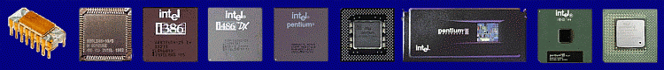
Part VI: Intel 8086, IBM's choice (1978)
. . . . . . . . . . . . . . . . .
The Intel 8086 was based on the design of the 8080/8085
(source compatible with the 8080)
with a similar register set, but was expanded to 16 bits. The Bus Interface Unit
fed the instruction stream to the Execution Unit through a 6 byte prefetch
queue, so fetch and execution were concurrent - a primitive form of pipelining
(8086 instructions varied from 1 to 4 bytes).
It featured four 16 bit general registers, which could also be accessed as
eight 8 bit registers, and four 16 bit index registers (including the stack
pointer). The data registers were often used implicitly by instructions,
complicating register allocation for temporary values. It featured 64K 8-bit I/O
(or 32K 16-bit) ports and fixed vectored interrupts. There were also four segment
registers that could be set from index registers.
The segment registers allowed the CPU to access 1 meg of memory through an
odd process. Rather than just supplying missing bytes, as most segmented
processors, the 8086 actually added the segment registers ( X 16, or shifted
left 4 bits) to the address. As a strange result of this unsuccessful attempt at
extending the address space without adding address bits, it was possible to have
two pointers with the same value point to two different memory locations, or two
pointers with different values pointing to the same location, and limited
typical data structures to less than 64K. Most people consider this a brain
damaged design.
Although this was largely acceptable for assembly language, where control of
the segments was complete (it could even be useful then), in higher level
languages it caused constant confusion (ex. near/far pointers). Even worse, this
made expanding the address space to more than 1 meg difficult. The 80286 (1982?)
expanded the design to 32 bits only by adding a new mode (switching from 'Real'
to 'Protected' mode was supported, but switching back required using a bug in
the original 80286, which then had to be preserved) which greatly increased the
number of segments
by using a 16 bit selector for a 'segment descriptor', which contained the
location within a 24 bit address space, size (still less than 64K), and
attributes (for Virtual Memory support) of a segment.
But all memory access was still restricted to 64K segments until the 80386
(1985), which included much improved addressing: base reg + index reg * scale
(1, 2, 4 or 8 bits) + displacement (8 or 32 bit constant = 32 bit address (in
the form of paged segments (using six 16-bit segment registers), like the IBM
S/360 series, and unlike the Motorola
68030). It also had several processor modes (including separate paged and
segmented modes) for compatibility with the previous awkward design. In fact,
with the right assembler, code written for the 8008
can still be run on the most recent Pentium Pro. The 80386 also added an MMU,
security modes (called "rings" of privledge - kernal, system services,
application services, applications) and new op codes in a fashion similar to the
Z-80
(and Z-280).
The 80486 (1989) added full pipelines, single on chip 8K cache, integrated
FPU (based on the eight element 80-bit stack-oriented FPU in the 80387 FPU), and
clock doubling versions (like the Z-280).
The Pentium (late 1993) was superscalar (up to two instructions at once in dual
integer units and single FPU) with separate 8K I/D caches.
The Pentium was the name Intel gave the 80586 version because it could not
legally protect the name "586" to prevent other companies from using it - and in
fact, the Pentium compatible CPU from NexGen is called the Nx586 (early 1995).
Due to its popularity, the 80x86 line has been the most widely cloned
processors, from the NEC V20/V30 (slightly faster clones of the 8088/8086 (could
also run 8085 code)), AMD and Cyrix clones of the 80386 and 80486, to versions
of the Pentium within less than two years of its introduction.
Interestingly, the old architecture is such a barrier to improvements that
most of the Pentium compatible CPUs (NexGen Nx586/Nx686, AMD K5), and even the
"Pentium Pro" (Pentium's successor, late 1995) don't clone the Pentium, but
emulate it with specialized hardware decoders which convert Pentium instructions
to RISC-like instructions which are executed on specially designed superscalar
RISC cores faster than the Pentium itself (the Cyrix/IBM 6x86 (early 1996) still
directly executes 80x86 instructions in two pipelines, but partly out
of order, making it faster than a Pentium). Intel also uses BiCMOS in the
Pentium and Pentium Pro to achieve clock rates competitive with CMOS RISC
processors (the Pentium P55C (early 1997) version will be a pure CMOS
design).
Persistant rumours that IBM was developing hardware to translate Pentium
instructions for the PowerPC
as part of the PowerPC
615 CPU eventually died.
The Pentium Pro (code named "P6") is a 1 or 2-chip (CPU plus 256K or 512K L2
cache - I/D L1 cache (8K each) is on the CPU), 14-stage superpipelined
processor. It uses extensive multiple branch prediction and speculative
execution via register
renaming. Three decoders (one for complex instructions, two for simpler ones
(four or fewer micro-ops)) each decode one 80x86 instruction into micro-ops (one
per simple decoder + up to four from the complex decoder = three to six per
cycle). Up to five (usually three) micro-ops can be issued in parallel and out
of order (six units - FPU, 2 integer, 2 address, 1 load/store), but are held
and retired (results written to registers or memory) as a group to prevent an
inconsistant state (equivalent to half an instruction being executed when an
interrupt occurs, for example). 80x86 instructions may produce several micro-ops
in CPUs like this (and the Nx586 and AMD K5), so the actual instruction rate is
lower. In fact, due to problems handling instruction alignment in the Pentium
Pro, emulated 16-bit instructions execute slower than on a Pentium.
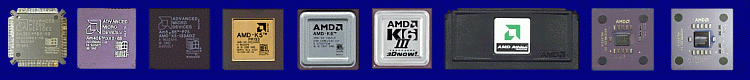
The AMD K5 translates 80x86 code to ROPs (RISC OPerations), which execute on
a RISC core based on the superscalar AMD 29K.
Up to four ROPs can be dispatched to six units (two integer, one FPU, two
load/store, one branch unit), and five can be retired at a time. The complexity
led to low clock speeds for the K5, prompting AMD to buy NexGen and integrate
its designs for the next generation K6.
The NexGen/AMD Nx586 (late 1994) is unique by being able to execute its
micro-ops (called RISC86 code) directly, allowing optimised RISC86 programs to
be written which are faster than an equivalent x86 program would be, but this
feature is seldom used. It also features two 16K I/D L1 caches, a dedicated L2
cache bus (like that in the Pentium Pro 2-chip module) and an off-chip FPU
(either separate chip, or later as in 2-chip module).
The Nx586 sucessor, the K6 (expected early 1996) actually has three caches -
32K each for data and instructions, and a half-size 16K cache containing
instruction decode information. It also brings the FPU on-chip and eliminates
the dedicated cache bus of the Nx586, allowing it to be pin-compatible with the
P54C model Pentium. Another decoder is added (two complex decoders, compared to
the Pentium Pro's one complex and two simple decoders) producing up to four
micro-ops and issuing up to six (to seven units - load, store, complex/simple
integer, FPU, branch, multimedia) and retiring four per cycle.
AMD has licensed the MMX (initially reported as MultiMedia eXtension, but
later said by Intel to mean Matrix Math eXtension) instructions that Intel has
developed for its own (Pentium and Pro) CPUs. MMX is very similar to the SPARC
VIS or HP-PA
MAX instructions) - they perform integer operations on groups of 8, 16, or
32 bit words, using the 80 bit FPU stack elements as eight 64 bit registers
(switching between FPU and MMX modes as needed - it's very difficult to use them
as a stack and as MMX registers at the same time). The Pentium P55C (January
1997) is the first Intel CPU to include MMX instructions, and Cyrix intends to
clone these instructions in its M2 CPU.
Intel, with partner Hewlett-Packard, has begun development of a next
generation 64-bit processor (code named Merced/Tahoe, compatible with the 80x86
in some versions, possibly with a hardware or software translater), apparently
based on Very Long Instruction Word technology, which may let the 80x86
architecture finally fade away.
So why did IBM chose the 8086 series when most of the alternatives were so
much better? Apparently IBM's own engineers wanted to use the 68000,
and it was used later in the forgotten IBM Instruments 9000 Laboratory Computer,
but IBM already had rights to manufacture the 8086, in exchange for giving Intel
the rights to its bubble
memory designs. Apparently IBM was using 8086s in the IBM Displaywriter word
processor.
Other factors were the 8-bit 8088 (1979) version, which could use existing
low cost 8085-type
components, and allowed the computer to be based on a modified 8085
design. 68000
components were not widely available, though it could use 6800
components to an extent. After the failure and expense of the IBM 5100
(1974/5/6? - their first attempt at a peronal computer - discrete random logic
CPU with no bus, built in BASIC and APL as the OS), cost was a large factor in
the design of the PC.
Intel bubble
memory was on the market for a while, but faded away as better and cheaper
memory technologies arrived.
Section Four: Unix and RISC, a New Hope
Part I: TRON, between the ages (1987) . .
TRON stands for The Real-time Operating Network, and was a grand scheme
devised by Japanese electronics firms to design a unified architecture for
computer systems from the CPU, to operating systems, to large scale networks. It
was designed just as RISC architectures were set to rise, but retained the CISC
design philosophies - it could be considered a last gasp, though that doesn't do
justice to the intent behind the design and its part in the TRON
architecture.
The basic design is scalable, from 32 to 48 and 64 bit designs, with 16
general purpose registers. It is a CISC instruction set, but an elegant one. One
early design was the Mitsubishi M32 (mid 1987), which optimised the simple and
often used TRON instructions, much like the 80486
and 68040
did. It featured a 5 stage pipeline, dynamic branch prediction with a target
branch buffer similar to that in the AMD 29K.
It also featured an instruction prefetch queue, but being a prototype, had no
MMU support or FPU.
Commercial versions such as the Gmicro/200 (and other Gmicro/) from Fujitsu
and Toshiba Tx1 were also introduced, but didn't catch on in the non-Japanese
market. In addition, many RISC designers (Sun, MIPS) licensed their (faster)
designs openly to Japanese companies. TRON's promise of a unified architecture
(when complete) was less important to companies than raw performance and
immediate compatibility (Unix, MS-DOS, Macintosh), and has not yet become
significant in the industry, though TRON operating system development continues
as an embedded distributed operating system (such as Intelligent House projects)
implemented on non-TRON CPUs.
Part II: SPARC, an extreme windowed RISC (1987) . .
SPARC, or the Scalable (originally Sun) Processor ARChitecture was designed
by Sun Microsystems for their own use. Sun was a maker of workstations, and used
standard 68000-based
CPUs and a standard operating system, Unix. Research versions of RISC processors
had promised a major step forward in speed [See Appendix
A], but existing manufacturers were slow to introduce a RISC type processor,
so Sun went ahead and developed its own (based on Berkeley's
design). In keeping with their open philosophy, they licensed it to other
companies, rather than manufacture it themselves.
SPARC was not the first RISC processor. The AMD
29000 (see below) came before it, as did the MIPS
R2000 (based on Stanford's
experimental design) and Hewlett-Packard
PA-RISC CPU, among others. The SPARC design was radical at the time, even
omitting multiple cycle multiply and divide instructions (added in later
versions), using single-cycle "step" instructions instead, while most RISC CPUs
were more conventional.
SPARC usually contains about 128 or 144 registers, (CISC designs typically
had 16 or less). At each time 32 registers are available - 8 are global, the
rest are allocated in a 'window' from a stack of registers. The window is moved
16 registers down the stack during a function call, so that the upper and lower
8 registers are shared between functions, to pass and return values, and 8 are
local. The window is moved up on return, so registers are loaded or saved only
at the top or bottom of the register stack. This allows functions to be called
in as little as 1 cycle. Like most RISC processors, global register zero is
wired to zero to simplify instructions, and SPARC is pipelined for performance
(a new instruction can start execution before a previous one has finished), but
not as deeply as others. Also like previous processors, a dedicated CCR holds
comparison results.
SPARC is 'scalable' mainly because the register stack can be expanded (up to
512, or 32 windows), to reduce loads and saves between functions, or scaled down
to reduce interrupt or context switch time, when the entire register set has to
be saved. Function calls are usually much more frequent than interrupts, so the
large register set is usually a plus, but compilers now can usually produce code
which uses a fixed register set as efficiently as a windowed register set across
function calls.
SPARC is not a chip, but a specification, and so there are various designs of
it. It has undergone revisions, and now has multiply and divide instructions.
Original versions were 32 bits, but 64 bit and superscalar versions were
designed and implemented (beginning with the Texas Instruments SuperSparc in
late 1992), but performance lagged behind other RISC and even Intel
80x86 processors until the UltraSPARC (late 1995) from Texas Instruments and
Sun, and superscalar HAL/Fuji SPARC64 multichip CPU.
The UltraSPARC is a 64-bit superscalar processor which can issue up to four
instructions at once (but not out
of order) to any of nine units: two integer units, two of the five floating
point/graphics units, the branch and load/store unit. The UltraSparc also added
a block move instruction which bypasses the caches (2-way 16K instr, 16K direct
mapped data), to avoid disrupting it, and specialized pixel operations (VIS -
the Visual Instruction Set) which can operate in parallel on 8, 16, or 32-bit
integer values packed in a 64-bit floating point register (for example, four 8 X
16 -> 16 bit multiplications in a 64 bit word, a sort of simple SIMD/vector
operation. More extensive than the Intel
MMX instructions, or earlier HP
PA-RISC MAX and Motorola
88110 graphics extensions, VIS also includes some 3D to 2D conversion, edge
processing and pixes distance (for MPEG, pattern-matching support).
The HAL/Fuji SPARC64 can issue up to four in order instructions
simultaneously to four buffers, then to four integer, two floating point, two
load/store, and the branch unit, and may complete out of order (an instruction
completes when it finishes without error, is committed when all instructions
ahead of it have completed, and is retired when its resources are freed - these
are 'invisible' stages in the SPARC64 pipeline). A combination of register
renaming, a branch history table, and processor state storage (like in the
Motorola
88K) allow for speculative
execution while maintaining precise exceptions/interrupts (renamed
integer, floating, and CC registers - trap levels are also renamed
and can be entered speculatively).
Part III: AMD 29000, a flexible register set (1987) . .
The AMD 29000 is another RISC CPU descended from the Berkeley
RISC design (and the IBM 801
project), as a modern successor to the earlier 2900
bitslice series (beginning around 1981). Like the SPARC
design that was introduced shortly later, the 29000 has a large set of registers
split into local and global sets. But though it was introduced before the SPARC,
it has a more elegant method of register management.
The 29000 has 64 global registers, in comparison to the SPARC's
eight. In addition, the 29000 allows variable sized windows allocated from the
128 register stack cache. The current window or stack
frame is indicated by a stack pointer (a modern version of the ISAR register
in the Fairchild
F8 CPU), a pointer to the caller's frame is stored in the current frame,
like in an ordinary stack (directly supporting stack languages like C, a
CISC-like philosophy). Spills and fills occur only at the ends of the cache, and
registers are saved/loaded from the memory stack. This allows variable window
sizes, from 1 to 128 registers. This flexibility, plus the large set of global
registers, makes register allocation easier than in SPARC
(optimised stack operations also make it ideal for a stack-oriented interpreted
languages such as PostScript, making it popular as a laser printer
controller).
There is no special condition code register - any general register is used
instead, allowing several condition codes to be retained, though this sometimes
makes code more complex. An instruction prefetch buffer (using burst mode)
ensures a steady instruction stream. Branches to another stream can cause a
delay, so the first four new instructions are cached - next time a cached branch
(up to sixteen) is taken, the cache supplies instructions during the initial
memory access delay.
Registers aren't saved during interrupts, allowing the interrupt routine to
determine whether the overhead is worthwhile. In addition, a form of register
access control is provided. All registers can be protected, in blocks of 4, from
access. These features make the 29000 useful for embedded applications, which is
where most of these processors are used, allowing it at one point to claim the
title of 'the most popular RISC processor'. The 29000 also includes an MMU and
support for the 29027 FPU. The superscalar 29050 version in 1990 integrated a
redesigned FPU (4 instructions could be dispatched to execute out
of order and speculatively).
In late 1995 Advanced Micro Devices dropped development of the 29K in favour
of its more profitable clones of Intel
80x86 processors, although much of the development of the superscalar core
for a new AMD 29000 (including FPU designs from the 29050) was shared with the
'K5'
(1995) Pentium
compatible processor (the 'K5'
translates 80x86
instructions to RISC-style instructions, and dispatches up to five at once to
two integer units, one FPU, a branch and a load/store unit).
Part IV:Siemens 80C166, Embedded RISC with register windows. . .
The Siemens 80C166 was designed as a very low-cost embedded 8/16-bit RISC
processor, with RAM (1 to 2K) kept on-chip for lower cost. This leads to some
unusual versions of RISC features.
The 80C166 has sixteen 16 bit registers, with the lower eight usable as
sixteen 8 bit registers, which are stored in overlapping windows (like in the SPARC)
in the on-chip RAM (or register bank), pointed to by the Context Pointer (CP)
(similar to the SP in the AMD
29K). Unlike the SPARC,
register windows can overlap by a variable amount (controlled by the CP), and
the there are no spills or fills because the registers are considered part of
the RAM address space (like in the TMS
9900), and could even extend to off chip RAM. This eliminates wasted
registers of SPARC
style windows.
Address space (18 to 24 bits) is segmented (64K code segments with a separate
code segment register, 16K data segments with upper two bits of 16 bit address
selecting one of four data segment registers).
The 80C166 has 32 bit instructions, while it's a 16 bit processor (compared
to the Hitachi
SH, which is a 32 bit CPU with 16 bit instructions). It uses a four stage
pipeline, with a limited (one instruction) branch cache.
Part V: MIPS R2000, the other approach. (June 1986) . . . . . . .
The R2000 design came from the Stanford
MIPS project, which stood for Microprocessor without Interlocked Pipeline
Stages [See Appendix
A], and was arguably the first commercial RISC processor (other candidates
are the ARM and
IBM
ROMP used in the IBM PC/RT workstation, which was designed around 1981 but
delayed until 1986). It was intended to simplify processor design by eliminating
hardware interlocks between the five pipeline stages. This means that only
single execution cycle instructions can access the thirty two 32 bit general
registers, so that the compiler can schedule them to avoid conflicts. This also
means that LOAD/STORE and branch instructions have a 1 cycle delay to account
for. However, because of the importance of multiply and divide instructions, a
special HI/LO pair of multiply/divide registers exist which do have hardware
interlocks, since these take several cycles to execute and produce scheduling
difficulties.
Like the AMD
29000 and DEC
Alpha, the R2000 has no condition code register considering it a potential
bottleneck. The PC is user readable. The CPU includes an MMU unit that can also
control a cache, and the CPU was one of the first which could operate as a big
or little endian processor. An FPU, the R2010, is also specified for the
processor.
Newer versions included the R3000 (1988), with improved cache control, and
the R4000 (1991) (expanded to 64 bits and is superpipelined (twice as many
pipeline stages do less work at each stage, allowing a higher clock rate and
twice as many instructions in the pipeline at once, at the expense of increased
latency when the pipeline can't be filled, such as during a branch, (and
requiring interlocks added between stages for compatibility, making the original
"I" in the "MIPS" acronym meaningless))). The R4400 and above integrated the FPU
with on-chip caches. The R4600 and later versions abandoned superpipelines.
The superscalar R8000 (1994) was optimised for floating point operation,
issuing two integer or load/store operations (from four integer and two
load/store units) and two floating point operations simultaneously (FP
instructions sent to the independent R8010 floating point coprocessor (with its
own set of thirty-two 64-bit registers and load/store queues)).
The R10000 version (early 1996) added multiple FPU units, as well as almost
every advanced modern CPU feature, including separate 2-way I/D caches (32K
each) plus on-chip secondary controller (and high speed 8-way split transaction
bus (up to 8 transactions can be issued before the first completes)),
superscalar execution (load four, dispatch five instructions (may be out
of order) to any of two integer, two floating point, and one load/store
units), dynamic register
renaming (thirty two integer and floating point rename registers), and an
instruction cache where instructions are partially decoded when loaded into the
cache, simplifying the processor decode (and register
rename/issue) stage. This technique was first implemented in the AT&T
CRISP/Hobbit CPU, described later.
The 2-way (int/float) superscalar R5000 (January, 1996) was added to fill the
gap between R4600 and R10000, without any fancy features (out of order or branch
prediction buffers). For embedded applications, MIPS and LSI Logic added a
compact 16 bit instruction set which can be mixed with the 32 bit set (same as
the ARM
Thumb 16 bit extension), implemented in a CPU called TinyRISC (October
1996), as well as MDMX (MIPS Digital Multimedia Extensions, announced October
1996)). MDMX adds parallel floating point (two 32 bit fields in 64 bit
registers) operations (compared to similar HP MAX
integer extensions), but also adds a 192 bit accumulator
for multimedia instructions. Future versions are expected to add Java
virtual machine support.
Part VI: Hewlett-Packard PA-RISC, a conservative RISC (Oct 1986) . . . . . .
A design typical of many RISC processors, the PA-RISC (Precision
Architecture, originally code-named Spectrum) was designed to replace older
processors in HP-3000 MPE minicomputers, and Motorola
680x0 processors in the HP-9000 HP/UX Unix minicomputers and workstations.
It has an unusually large instruction set for a RISC processor (including a
conditional skip instruction, similar in concept to the condition bits in the ARM
processor), partly because initial design took place before RISC philosophy was
popular, and partly because careful analysis showed that performance benefited
from the instructions chosen - in fact, version 1.1 added new multiple operation
instructions combined from frequent instruction sequences, and HP was among the
first to add multimedia instructions (the MAX-1 and MAX-2 instructions, similar
to Sun
VIS or Intel
MMX). Despite this, it's a simple design - the entire original CPU had only
115,000 transistors, less than twice the much older 68000.
Much of the RISC philosophy was independently invented at HP from lessons
learned from FOCUS (pre 1984), HP's (and the world's) first fully 32 bit
microprocessor. It was a huge (at the time) 450,000 transistor chip with a stack
based instruction set, described as "essentially a gigantic microcode
ROM with a simple 32 bit data path bolted to its side". Performance wasn't
spectacular, but it was used in a pre-Unix workstation from HP.
It's almost the cannonical RISC design, similar except in details to most
other mainstream RISC processors like the Fairchild/Intergraph
Clipper (1986), and the Motorola
88K in particular. It has a 5 stage pipeline, which (unlike early MIPS
(R2000) processors) had hardware interlocks from the beginning for
instructions which take more than one cycle, as well as result forwarding (a
result can be used by a previous instruction without waiting for it to be stored
in a register first).
It is a load/story architecture, originally with a single instruction/data
bus, later expanded to a Harvard
architecture (separate instruction and data buses). It has thirty-two 32-bit
integer registers (GR0 wired to constant 0, GR31 used as a link register for
procedure calls), with seven 'shadow registers' which preserve the contents of a
subset of the GR set during fast interrupts (also like ARM),
and thirty-two 64-bit floating point registers (also as sixty-four 32-bit and
sixteen 128-bit), in an FPU (which could execute a floating point instruction
simultaneously, from the Apollo-designed Prism architecture (1988?) after
Hewlett-Packard acquired the company). Later versions (the PA-RISC 7200 in 1994)
added a second integer unit (still dispatching only two instructions at a time
to any of the three units). Addressing originally was 48 bits, and expanded to
64 bits, using a segmented
addressing scheme.
The PA-RISC 7200 also included a tightly integrated cache and MMU, a high
speed 64-bit 'Runway' bus, and a fast but complex fully associative 2KB on-chip
assist cache, between the simpler direct-mapped data cache and main memory,
which reduces thrashing (repeatedly loading the same cache line) when two memory
addresses are aliased (mapped to the same cache line). Instructions are
predecoded into a separate instruction cache (like the AT&T
CRISP/Hobbit).
The PA-RISC 8000 (April 1996), intended to compete with the R10000,
UltraSparc,
and others) expands the registers and architecture to 64 bits (eliminating
segments), and adds aggressive superscalar design which includes issuing 4
instructions to ten functional units, out
of order execution and dynamic reordering (fifty six rename registers) with
a deeper pipeline, and speculative
execution of branches (the same features as the R10000).
Although typically sporting fewer of the advanced (and promised) features of
competing CPUs designs, a simple elegant design and effective instruction set
has kept PA-RISC performance among the best in its class (of those actually
available at the same time) since its introduction.
HP pioneered the addition of multimedia instructions with the MAX-1
(Multimedia Acceleration eXtension) extensions in the PA-7100LC (pre-1994) and
64-bit (version 2.0) MAX-2 extensions in the PA-8000, which allowed parallel
operations on two or four 16-bit subwords in 32-bit or 64-bit integer registers
(this only required selectively dropping the carry bit between subwords, adding
only 0.1 percent to the PA-8000 CPU area, while using the FPU registers like Sun's
VIS and Intels
MMX do would have required duplicating ALU functions. 8 and 32-bit support,
multiplication, and complex instructions were also left out in favour of
powerful 'mix' and 'permute' packing/unpacking operations).
In the future Hewlett-Packard plans to pursue a "post-VLIW" (Very Long
Instruction Word) design in conjunction with Intel, possibly expanding on the
idea of MAX or MMX
operations. Some of the newer CPUs which execute Intel
80x86 instructions (The AMD
'K5' and NexGen
Nx586 (late 1994), for example) treat 80x86
instructions as VLIW instructions, decoding them into RISC-like instructions and
executing several concurrently.
Part VII: Motorola 88000, Late but elegant (mid 1988) . . . .
The Motorola 88000 (originally named the 78000) is a 32 bit processor, one of
the first RISC CPUs based on a Harvard
architecture (the same as the Fairchild/Intergraph
Clipper C100 (1986) beat it by 2 years). Each bus has a separate cache, so
simultaneous data and instruction access doesn't conflict. Except for this, it
is similar to the Hewlett
Packard Precision Architecture (HP/PA) in design (including many
control/status registers only visible in supervisor mode), though the 88000 is
more modular, has a small and elegant instruction set, and lacks segmented
addressing (limiting addressing to 32 bits, vs. 64 bits). The 88200 MMU unit
also provides dual caches (including multiprocessor support) and MMU functions
for the 88100 CPU (like the Clipper).
The 88110 includes caches and MMU on-chip.
The 88000 has thirty-two 32 bit user registers, with up to 8 distinct
internal function units - an ALU and a floating point unit (sharing the single
register set) in the 88100 version, multiple ALU and FPU units (with thirty-two
80-bit FPU registers) and two-issue instuctions were added to the 88110 to
produce one of the first superscalar designs (following the 320xx
Swordfish). Other units could be designed and added to produce custom
designs for customers, and the 88110 added a graphics/bit unit which pack or
unpack 4, 8 or 16-bit integers (pixels) within 32-bit words, and multiply packed
bytes by an 8-bit value. But it was introduced late and never became as popular
in major systems as the MIPS
or HP
processors. Development (and performance) has lagged as Motorola favoured
the PowerPC
CPU, coproduced with IBM.
Like the most modern processors, the 88000 is pipelined (with interlocks),
and has result forwarding (in the 88110 one ALU can feed a result directly into
another for the next cycle). Loads and saves in the 88110 are buffered so the
processor doesn't have to wait, except when loading from a memory location still
waiting for a save to complete. The 88110 also has a history buffer for speculatively
executing branches and to make interrupts 'precise' (they're imprecise in
the 88100). The history buffer is used to 'undo' the results of speculative
execution or to restore the processor to 'state' when the interrupt occurred - a
1 cycle penalty, as opposed to 'register
renaming' which buffers results in another register and either discards or
saves it as needed, without penalty.
Part VIII: Fairchild/Intergraph Clipper, An also-ran (1986) . .
The Clipper C100 was developed by Fairchild, later sold to workstation maker
Intergraph, which took over chip development (produced the C300 in 1988) until
it decided it couldn't compete in processor technology, and switched to Intel
80x86-based processors (Fairchild itself was bought by National
Semiconductor).
The C100 was a three-chip set like the Motorola
88000 (but predating it by two years), with a Harvard
architecture CPU and separate MMU/cache chips for instruction and data. It
differed from the 88K and
HP
PA-RISC in having sixteen 32-bit user registers and eight 64-bit FPU
registers, rather than the more common thirty-two.
The only other distinguishing features of the Clipper are a bank of sixteen
supervisor registers which completely replace the user registers, (the ARM
replaces half the user registers on an FIRQ interrupt) and the addition of some
microcode
instructions like in the Intel
i960.
Part IX: Acorn ARM, RISC for the masses (1986) . . . .
ARM (Advanced RISC Machine, originally Acorn RISC Machine) is often praised
as one of the most elegant modern processors in existence. It was meant to be
"MIPs for the masses", and designed as part of a family of chips (ARM - CPU,
MEMC - MMU and DRAM/ROM controller, VIDC - video and DAC, IOC - I/O, timing,
interrupts, etc), for the Archimedes home computer (multitasking OS, windows,
etc). It's made by VLSI Technologies Inc, and based partly on the Berkeley
experimental RISC design. It is simple, has a short 3-stage pipeline, and it can
operate in big- or little-endian mode.
The original ARM (ARM1, 2 and 3) was a 32 bit CPU, but used 26 bit
addressing. The newer ARM6xx spec is completely 32 bits. It has user,
supervisor, and various interrupt modes (including 26 bit modes for ARM2
compatibility). The ARM architecture has sixteen registers (including user
visible PC as R15) with a multiple load/save instruction, though many registers
are shadowed in interrupt modes (2 in supervisor and IRQ, 7 in FIRQ) so need not
be saved, for fast response. The instruction set is reminiscent of the 6502,
used in Acorns earlier computers.
A unique feature of ARM is that every instruction features a 4 bit condition
code (including 'never execute', not officially recommended). Another bit
indicates whether the instruction should set condition codes, so intervening
instructions don't change them. This easily eliminates many branches and can
speed execution. Another unique and useful feature is a barrel shifter which
operates on the second operand of most ALU operations, allowing shifts to be
combined with most operations (and index registers for addressing), effectively
combining two or more instructions into one.
These features make ARM code both dense (unlike most RISC processors) and
efficient, despite the relatively low clock rate and short pipeline - it is
roughly equivalent to a much more complex 80486
in speed. And like the Motorola
Coldfire, ARM has developed a low cost 16-bit version called Thumb, which
recodes a subset of ARM CPU instructions into 16 bits (decoded to native 32-bit
ARM instructions without penalty - similar to the CISC decoders in the newest 80x86
compatible and 68060
processors, except they decode native instructions into a newer one, while Thumb
does the reverse). Thumb programs can be 30-40% smaller than already dense ARM
programs. Native ARM code can be mixed with Thumb code when the full instruction
set is needed.
The ARM series consists of the ARM6 CPU core (35,000 transistors, which can
be used as the basis for a custom CPU) the ARM60 base CPU, and the ARM600 which
also includes 4K 64-way set-associative cache, MMU, write buffer, and
coprocessor interface (for FPU). A newer version, the ARM7 series (Dec 1994),
increases performance by optimising the multiplier, and adding DSP extensions
including 32 bit and 64 bit multiply and multiply/accumulate instructions
(operand data paths lead from registers through the multiplier, then the shifter
(one operand), and then to the integer ALU for up to three independent
operations). It also doubles cache size to 8K, includes embedded In Circuit
Emulator (ICE) support, and raises the clock rate significantly.
The ARM CPU was chosen for the Apple Newton handheld system because of its
speed, combined with the low power consumption, low cost and customizable design
(the ARM610 version used by Apple includes a custom MMU supporting object
oriented protection and access to memory for the Newton's NewtOS). DEC has also
licensed the architecture, and has developed the SA-110 (StrongARM) (February
1996), running a 5-stage pipeline at 100 to 233MHz (using only 1 watt of power),
with 5-port register file, faster multiplier, single cycle shift-add, and Harvard
architecture (16K each 32-way I/D caches). To fill the gap between ARM7 and
DEC StrongARM, ARM also developed the ARM8/800 which includes many StrongARM
features.
An experimental asynchronous version of the ARM6 (operates without an
external or internal clock signal) called AMULET has been produced by Steve
Furber's research group at Manchester university. The first version (AMULET1,
early 1993) is about 70% the speed of a 20MHz ARM6 on average (using the same
fabrication process), but simple operations (multiplication is a big win at up
to 3 times the speed) are faster (since they don't need to wait for a clock
signal to complete). AMULET2e (93K transistor AMULET2 core plus four 1K fully
associative cache blocks) is expected to be 30% faster (1/2 the performance of a
75MHz ARM810 using same fabrication), use less power, and includes features such
as branch prediction, due in late 1996.
Part X: Hitachi SuperH series, Embedded, small, economical (1992) . . .
Although the TRON
project produced processors competitive in performance (Fujitsu's(?) Gmicro/500
CISC CPU (1993) was faster and used less power than a Pentium),
the idea of a single standard processor never caught on, and newer concepts
(such as RISC features) overtook the TRON
design.
The Hitachi SH series is designed for the embedded marked, and so is similar
to the ARM
architecture in many ways. It's a 32 bit processor, but with a 16 bit
instruction format (different than Thumb, which is a 16 bit encoding of a subset
of ARM 32
bit instructions, or the NEC V800 series, which mixes 16 and 32 bit instruction
formats), and has sixteen general purpose registers and a load/store
architecture (again, like ARM).
This results in a very high code density, similar to the 680x0
and 80x86
CPUs, and about half that of the PowerPC.
Because of the small instruction size, there are no immediate load instruction,
but a PC-relative addressing mode is supported to load 32 bit values (unlike ARM or
PDP-11,
the PC is not otherwise visible).
The SH3 design (1996) also has a Multiply ACcumulate (MAC) instruction, and
MACH/L (high/low word) registers, and includes an MMU and 2K to 8K of unified
cache.
The SH is used in many of Hitachi's own products as well as others, and is
most prominently featured in the Sega Saturn video game system (which uses two
SH2 CPUs).
Section Five: Born Beyond Scalar
Part I: Intel 960, Intel quietly gets it right (1987 or 1988?) . . . .
Largely obscured by the marketing hype surrounding the Intel
80860, the 80960 was actually an overall better processor, and replaced the
AMD
29K series as "the world's most popular embedded RISC" until 1996. The 960
was aimed for the high end embedded market (it included multiprocessor and
debugging support, and strong interrupt/fault handling, but lacked MMU support),
while the 860 was
intended to be a general purpose processor (the name 80860
echoing the popular 8086).
Although the first implementation was not superscalar, the 960 was designed
to allow dispatching of instructions to multiple (undefined, but generally
including at least one integer) execution units, which could include internal
registers (such as the four 80 bit registers in the floating point unit (32, 64,
and 80 bit IEEE operations)) - the 960 CA version (1989) was superscalar. There
are sixteen 32 bit global registers which can be shared by all excution units
and sixteen register "caches" - similar to the SPARC
register windows, but not overlapping (originally four banks). It's a RISC-based
load/store Harvard
architecture (32-bit flat addressing), but has some complex microcoded
instructions (such as CALL/RET). There are also thirty-two 32 bit special
function registers.
It's a very clean embedded architecture, not designed for high level
applications, but very effective and scalable - something that can't be said for
all Intel's processor designs.
Part II: Intel 860, "Cray on a Chip" (late 1988?) . . .
The Intel 80860 was an impressive chip, able at top speed to perform close to
66 MFLOPS at 33 MHz in real applications, compared to a more typical 5 or 10
MFLOPS for other CPUs of the time. Much of this was marketing hype, and it never
become popular, lagging behind most newer CPUs and Digital Signal Processors in
performance.
The 860 has several modes, from regular scaler mode to a superscalar mode
that executes two instructions per cycle and a user visible pipeline mode
(instructions using the result register of a multi-cycle op would take the
current value instead of stalling and waiting for the result). It can use the 8K
data cache in a limited way as a small vector register (like those in
supercomputers). The unusual cache uses virtual addresses, instead of physical,
so the cache has to be flushed any time the page tables changes, even if the
data is unchanged. Instruction and data busses are separate, with 4 G of memory,
using segments.
It also includes a Memory Management Unit for virtual storage.
The 860 has thirty two 32 bit registers and thirty two 32 bit (or sixteen 64
bit) floating point registers. It was one of the first microprocessors to
contains not only an FPU as well as an integer ALU, and also included a 3-D
graphics unit (attached to the FPU) that supports lines drawing, Gouraud
shading, Z-buffering for hidden line removal, and operations in conjunction with
the FPU. It was also the first able to do an integer operation, and a (unique at
the time) multiply and add floating point instruction, for the equivalent of
three instructions, at the same time.
However actually getting the chip at top speed usually requires using
assembly language - using standard compilers gives it a speed closer to other
processors. Because of this, it was used as a coprocessor, either for graphics,
or floating point acceleration, like add in parallel units for workstations.
Another problem with using the Intel 860 as a general purpose CPU is the
difficulty handling interrupts. It is extensively pipelined, having as many as
four pipes operating at once, and when an interrupt occurs, the pipes can spill
and lose data unless complex code is used to clean up. Delays range from 62
cycles (best case) to 50 microseconds (almost 2000 cycles).
Part III: IBM RS/6000 POWER chips (1990) . . .
When IBM decided to become a real part of the workstation market (after its
unsuccessful PC/RT
based on the ROMP
processor), it decided to produce a new innovative CPU, based partly on the 801
project that pioneered RISC theory. RISC normally stands for Reduced Instruction
Set Computer, but IBM calls it Reduced Instruction Set Cycles, and implemented a
relatively complex processor with more high level instructions than most CISC
processors. They ended up with was a CPU (POWER1) that initially contained five
or seven separate chips - the branch unit, fixed point unit, floating point
unit, and either two or four cache chips (separate data and instruction cache).
Some PowerPC versions (co-developed by IBM, Apple, and Motorola as a successor
to both the Motorola
68000 and Intel
80x86) have a unified on-chip cache (32K in the 601), newer versions have
split I/D caches. PowerPC versions also have a simplified instruction set,
emulating the older instructions if necessary.
The branch unit is the heart of the CPU, and enables multiple instructions
(up to four in the original POWER1, more commonly two or three) to be executed
at once. It contains the condition code register, a loop register (can decrement
and branch on zero with no penalty - a feature usually only found on DSPs like
the TMS320C30),
and performs branches. The condition code register has eight fields - in POWER1
two were reserved for the fixed and floating point units, the other six could be
set separately (or combined from several instructions), and can be checked
several instructions later. It also dispatches multiple instructions (out
of order if possible) to available execution units (each unit has a buffer
allowing instructions to be dispatched to a unit still executing a complex
instruction).
The branch unit can speculatively
take branches (using a prediction bit in the POWER1 and PowerPC 601 (1993), and
using dynamic prediction and a Branch History Table in the PowerPC 604 (mid
1995) and newer versions), dispatching instructions and then canceling them if
the branch is not taken (3 cycle maximum penalty) while buffering the other
instruction path to reduce latency. The branch unit also manages procedure calls
and returns on a program counter stack, allowing effective zero-cycle calls when
overlapped with other instructions. Finally, it handles interrupts (except
floating point exceptions) without software intervention.
The integer unit(s) perform integer operations, as well as some complex
string instructions in the POWER1 and 2 and 64-bit PowerPC-AS (mid 1996), and
loads and stores in the POWER1 and PowerPC 601 (newer versions added a separate
concurrent load/store unit). Most versions contain thirty two 32 bit registers
(the POWER1/2 design included a special MQ register for integer multiply/divides
(like the MIPS
HI/LO registers), but it was removed in PowerPC CPUs after the 601 as a
potential bottleneck), while the PowerPC 620 (delivered late, April 1996,
thenwithdrawn to make it faster) and AS registers are 64 bits (with appropriate
new instructions). The high end PowerPC-AS, intended for the AS/400 minicomputer
series, also has decimal arithmetic and string instructions (but only for 64-bit
instructions), and an interface for a matrix coprocessor (for possible future
RS/6000 workstations). All integer units can forward results needed by
subsequent instructions before the write stage occurs, and some versions
(PowerPC 603 and later) include extra registers which are renamed
for speculative
or out
of order instruction execution to prevent write conflicts, and make it
easier to discard the results of a canceled instruction. A reorder buffer in the
branch/dispatch unit tracks renamed
integer and floating point registers.
The floating point unit contains thirty two 64 bit registers and performs all
typical floating point operations (single or double precision in PowerPC, double
only in POWER1 and POWER2), including multiply/accumulate instructions and array
multiply and add. The registers are loaded and stored by the fixed point unit in
POWER1 and PowerPC 601, by the Load/Store unit in others (the multichip POWER2
has two dedicated floating point load/store units). The FPU also includes rename
registers. Like some other CPUs, floating point traps are imprecise because
of pipelining - normally, a trap bit is set on a floating point exception, and
software can test for the condition to generate a trap - or ignore it if its a
safe operation. For debugging, a slower precise trap mode is included.
Data buses range from 32 bits for early and low end versions to 256 bits
(plus ECC bits) for the high bandwidth POWER2 multichip CPU (late 1993 - 8
chips, 23 million transistors including 256K cache) which issues up to six
instructions and four simultaneous loads or stores. The PowerPC 601 used the Motorola
88000 microprocessor bus, more recent versions use PowerPC specific buses,
some with a 128 bit 'backside' bus (620 and later versions) used to access a L2
cache.
Overall the IBM POWER CPU is very powerful, reminiscent of mainframe designs,
which almost qualifies it as "Weird and Innovative", and violates the RISC
philosophy of simplicity and fewer instructions (at over a hundred (including
identical pairs where one implicitly sets the CC registers and the other
doesn't), versus only about 34 for the ARM and
52 for the Motorola
88000 (including FPU instructions)). The high complexity is very effective,
but also limits the clock rate of the designs - an interesting tradeoff
considering that a highly parallel 71.5 MHz POWER2 is faster than a 200MHz DEC Alpha
21064.
Very high clock rate (500MHz) BiCMOS 704 (based on a simplified 604 with only
one integer, one FPU, one load/store unit) is being developed (early 1997) by
Exponential Technology, expanding on the type of technology Intel found
necessary to keep its Pentium
and Pentium
Pro CPUs competitive. Embedded versions have also been introduced by IBM
(40x series) and Motorola (8xx and 50x series - ironically, Motorola now has a
MPC860 CPU with a future (on-chip communications support), in contrast to the Intel
i860).
Part IV: DEC Alpha, Designed for the future (1992) . . .
The DEC Alpha architecture is designed, according to DEC, for a operational
life of 25 years. Its main innovation is PALcalls (or writable instruction set
extension), but it is an elegant blend of features, selected to ensure no
obvious limits to future performance - no special registers, etc. The first
Alpha chip is the 21064.
Alpha is a 64 bit architecture (32 bit instructions) that doesn't support 8-
or 16-bit operations, but allows conversions, so no functionality is lost (Most
processors of this generation are similar, but have instructions with implicit
conversions). Alpha 32-bit operations differ from 64 bit only in overflow
detection. Alpha does not provide a divide instruction due to difficulty in
pipelining it. It's very much like the MIPS
R2000, including use of general registers to hold condition codes. However,
Alpha has an interlocked pipeline, so no special multiply/divide registers are
needed, and Alpha is meant to avoid the significant growth in complexity which
the R2000
family experienced as it evolved into the R8000
and R10000.
One of Alpha's roles is to replace DEC's two prior architectures - the MIPS-based
workstations and VAX
minicomputers (Alpha evolved from a VAX replacment project codenamed PRISM, not
to be confused with the Apollo
Prism acquired by Hewlett Packard). To do this, the chip provides both IEEE
and VAX 32
and 64 bit floating point operations, and features Privileged Architecture
Library (PAL) calls, a set of programmable (non-interruptable) macros written in
the Alpha instruction set, similar to the programmable microcode
of the Western
Digital MCP-1600 or the AMD
Am2910 CPUs, to simplify conversion from other instruction sets using a
binary translator, as well as providing flexible support for a variety of
operating systems.
Alpha was also designed for the future for a 1000-fold eventual increase in
performance (10 X by clock rate, 10 X by superscalar execution, and 10 X by
multiprocessing) Because of this, superscalar instructions may be reordered, and
trap conditions are imprecise (like in the 88100).
Special instructions (memory and trap barriers) are available to syncronise both
occurrences when needed (different from the POWER
use of a trap condition bit which is explicitly by software, but similar in
effect. SPARC
also has a specification for similar barrier instructions). And there are no
branch delay slots like in the R2000,
since they produce scheduling problems in superscalar execution, and
compatibility problems with extended pipelines. Instead speculative
execution (branch instructions include hint bits) and a branch cache are
used.
The 21064 was introduced with one integer, one floating point, and one
load/store unit. The 21164 (Early 1995) added one integer/load/store unit with
byte vector (multimedia-type) instructions (replacing the load/store unit) and
one floating point unit, and increased clock speed from 200 MHz to 300 MHz
(still roughly twice that of competing CPUs), and introduced the idea of a level
2 cache on chip (8K each inst/data level 1, 96K combined level 2). The 21264
(early 1997) expanded this to four integer units (two add/logic/shift/branch
(one also with multiply, one with multimedia) and two add/logic/load/store), two
different floating point units (one for add/div/square root and for multiply),
with the ability to load four, dispatch six, and retire eight instructions per
cycle (and for the first time including 40 integer and 40 floating point rename
registers and out
of order execution), at up to 500MHz. Multimedia extensions introduced with
the 21264 are simple, but include VIS-type
motion estimation (MPEG).
DEC's Alpha is in many ways the antithesis of IBM's
POWER design, which gains performance from complexity, and the expense of a
large transistor count, while the Alpha concentrates on the original RISC idea
of simplicity and a higher clock rate - though that also has its drawback, in
terms of very high power consumption.
Section Six: Weird and Innovative Chips
Part I: Intel 432, Extraordinary complexity (1980) . .
The Intel iAPX 432 was a complex, object oriented 32-bit processor that
included high level operating system support in hardware, such as process
scheduling and interprocess messaging. It was intended to be the main Intel
microprocessor (some said the 80286
was envisioned as a step between the 8086
and the 432, others claim the 8086
was to be the bridge to the 432, rushed through design when the 432 was late and
resulting in its many design problems). The 432 actually included four chips.
The GDP (processor) and IP (I/O controller) were introduced in 1980, and the BIU
(Bus Interface Unit) and MCU (Memory Control Unit) were introduced in 1983 (but
not widely). The GDP complexity was split into 2 chips (decode/sequencer and
execution units, like the Western
Digital MCP-1600), so it wasn't really a microprocessor.
The GDP was exclusively object oriented - normal linear memory access wasn't
allowed, and there was hardware support for data hiding, methods, inheritance,
late binding, and access protection, and it was promoted as being ideal for the
Ada programming language. To enforce this, permission and type checks for every
memory access (via a 2 stage segmentation)
slowed execution (despite cached segment tables). It supported up to 2^24
segments, each limited to 64K in size (within a 2^32 address space), but the
object oriented nature of the design meant that was not a real limitation. The
stack oriented design meant the GDP had no user data registers. Instructions
were bit encoded (and bit-aligned in memory), ranging from 6 bits to 321 bits
long (the T-9000
has variable length byte encoded/aligned instructions) and could be very
complex.
The BIU defined the bus, designed for multiprocessor support allowing up to
63 modules (BIU or MCU) on a bus and up to 8 independent buses (allowing memory
interleaving to speed access). The MCU did automatic parity checking and ECC
error correcting. The total system was designed to be fault tolerant to a large
degree, and each of these parts contributes to that reliability.
Despite these advanced features, the 432 didn't catch on. The main reason was
that it was slow, sometimes up to five or ten times slower than a 68000
or Intel's own 80286.
Part of this was the lack of local (user) data registers, or a data cache. Part
of this was the fault-tolerant BIU, which defined an (asynchronous protocol)
clocked bus that resulted in 25% to 40% of the access time being used by wait
states. The instructions weren't aligned on bytes or words, and took longer to
decode. In addition, the protections imposed on the objects slowed data access.
Finally, the implementation of the GDP on two chips instead of one produced a
slower product. However, the fact that this complex design was produced and bug
free is impressive.
Its high level architecture was similar to the Transputer
systems, but it was implemented in a way that was much slower than other
processors, while the T-414
wasn't just innovative, but much faster than other processors of the time.
The Intel
i960 is sometimes considered a successor of the 432 (also called "RISC
applied to the 432"), and does have similar hardware support for context
switching. This path came about indirectly through the 960 MC
designed for the BiiN machine, which was still very complex (it included many
i432 object-oriented ideas, including a tagged memory system).
Part II: Rekursiv, an object oriented processor .
The Rekursiv processor is actually a 4 chip processor motherboard, not a
microprocessor, but is neat. It was created by a Scottish Hi-Fi manufacturing
company called Linn, to control their manufacturing system. The owner (Ivor) was
a believer in automation, and had automated the company as much as possible with
Vaxes, but wasn't satisfied, so hired software experts to design a new system,
which they called LINGO. It was completely object oriented, like smalltalk (and
unlike C++, which allows object concepts, but handles them in a conventional
way), but too slow on the VAXes, so Linn commissioned a processor designed for
the language.
This is not the only processor designed specifically for a language that is
slow on other CPUs. Several specialized LISP processors, such as the Scheme-79
lisp processor, were created, but this chip is unique in its object oriented
features. It also manages to support objects without the slowness of the Intel
432.
The Rekursiv processor features a writable instruction set, and is highly
parallel. It uses 40 bits for objects, and 24 bit addressing, kind of. Memory
can't be addressed directly, only through the object identifiers (segments),
which are 40 bit tags. The hardware handles all objects in memory and on disk,
and swapping them to disk. It has no real program - all data and code/methods
are embedded in the objects, and loaded when a message is sent to them. There is
a page table which stores the object tags and maps them into memory.
There is a 64k area, arranged as 16k X 128 bit words, for microcode,
allowing an instruction set to be constructed on the fly. It can change for
different objects.
The CPU hardware creates, loads, saves, destroys, and manipulates objects.
The manipulation is accomplished with a standard AMD
29203 CPU, but the other parts are specially designed. It executes LINGO
entirely fast enough, and is a perfect match between language and CPU, but it
can execute more conventional languages, such as Smalltalk or C if needed -
possible simultaneously, as separate complete objects.
Unfortunately, Linn did not have the resources to pursue this very promising
(the prototype was "surprisingly easy" to implement) architecture.
Part III: TMS320C30, a popular DSP architecture (1988) . . . . . .
Digital Signal Processors can act as general purpose processors, but are
optimised for certain types of computation (such as signal processing involving
matrix computation), usually in embedded applications - resulting in designs
which are both somewhat weird and innovative, compared to general purpose CPUs
(although not when compared to other DSPs such as the TMS 320Cx0 - but this is a
CPU list, not a DSP list, so they go in this section). There is usually little
or no interrupt support, or memory management support.
The 320C30 is a 32 bit floating point DSP, based on the earlier 320C20/10 16
bit fixed point DSPs (1982). It has eight 40 bit extended precision registers R0
to R7 (32 bits plus 8 guard bits for floating, 32 bits for fixed), eight 32 bit
auxiliary registers AR0 to AR7 (used for pointers) with two separate arithmetic
units for address calculation, and twelve 32 bit control registers (including
status, an index register, stack, interrupt mask, and repeat block loop
registers).
It includes on chip memory in the form of one 4K ROM block, and two 1K RAM
blocks - each bus has its own bus, for a total of three (compared to one
instruction and one data bus in a Harvard
architecture), which essentially function as programer controlled caches.
Two arguments to the ALU can be from memory or registers, and the result is
written to a register, through a 4 stage pipeline.
The ALU, address controller and control logic are separate - much clearer in
the AT&T DSP32 and Motorola
56000 designs, and is even reflected in the MIPS
R8000 processor FPU and IBM
POWER architecture with its Branch Unit loop counter. The idea is to allow
the separate parts to operate as independently as possible (for example, a
memory access, pointer increment, and ALU operation), for the highest
throughput, so instructions accessing loop and condition registers don't take
the same path as data processing instructions.
The TMS320Cx0 series also includes the 320C8x (1994?), which has two or four
DSP cores on a single chip as well as a RISC CPU (thirty two 32-bit regs,
load/store, plus FPU) for control.
Part IV: Motorola DSP96002, an elegant DSP architecture . . . .
. . . . .
The 96002 is based on (and remaines software compatible with) the earlier
56000 24 bit fixed point DSP (most fixed points DSPs are 16 bit, but 24 bits
make it ideal for audio processing, without the high cost of floating point 32
bit DSPs). A 16 bit version (the 5616) was introduced later.
Like the TMS320C30,
the 96002 has a separate program memory (RAM in this case, with a bootstrap ROM
used to load the initial external program) and two blocks of data RAM, each with
a separate data and address busses. The data blocks can also be switched to ROM
blocks (such as sine and cosine tables). There's also a data bus for access to
external memory. Separate units work independently, with their own registers
(generally organised as three 32 bit parts of a single 96 bit register in the
96002 (where the '96' comes from).
The program control unit has a register containing 32 bit PC, status, and
operating mode registers, plus 32 bit loop address and 32 bit loop counter
registers (branches are 2 cycles, conditional branches are 3 cycles - with
conditional execution support), and a fifteen element 64 bit stack (with
separate 6 bit stack pointer).
The address generation unit has seven 96 bit registers, divided into three 32
bit (24 in the 56000/1) registers - R0-R7 address, N0-N7 offset, and M0-M7
modify (containing increment values) registers.
The Data Unit includes ten 96-bit floating point/integer registers, grouped
as two 96 bit accumulators (A and B = three 32 bit registers each: A2, A1, A0
and B2, B1, B0) and two 64 bit input registers (X and Y = two 32 bit registers
each: X1, X0 and Y1, Y0). Input registers are general purpose, but allow new
operands to be loaded for the next instruction while the current contents are
being used (accumulators are 8+24+24 = 56 bit in the 56000/1, where the '56'
comes from). The DSP96000 was one of the first to perform fully IEEE floating
point compliant operations.
The processor is not pipelined, but designed for single cycle independent
execution within each unit (actually this could be considered a three stage
pipeline). With multiple units and the large number of registers, it can perform
a floating point multiply, add and subtract while loading two registers,
performing a DMA transfer, and four address calculations within a two clock tick
processor cycle, at peak speeds.
The DSP56K and 680xx CPUs have been combined in one package in the Motorola
68456.
The DSP56K was part of the ill-fated NeXT system, as well as the lesser known
Atari Falcon (still made in low volumes for music buffs).
Part V: MISC M17: Casting Forth in Silicon[1] (pre 1988?) .
.
Forth is used widely for programming embedded systems because of its
simplicity and efficiency. It explicitly manipulates data on a stack, and so
defines a simple virtual machine architechture which makes programs independent
of the CPU - only the interpreter needs to be ported. Because of this, extra CPU
features are wasted when running Forth programs, and since cost reduction is
important to embedded systems, it's logical to want a simpler, cheaper CPU which
runs only Forth programs.
The M17 CPU wasn't the first Forth microprocessor (the Novix NC4000/4016
(1985?) came before), but the M17 is a good example of low cost Forth CPUs. It
featured two 16 bit stack pointers (Data and Return (subroutine) stacks), plus
three 16-bit top of stack data registers (X, Y, Z, plus an extra LastX which
could hold values popped from X). An I/O register buffered data during I/O while
the ALU operated concurrently. Finally, there was an Index register which
normally held the top element of the Return stack, but could also be used as a
loop counter, and a 6 instruction buffer (for short loops, like the Motorola
68010).
Address space was 64K, but external memory could be either a single bank or
up to five banks, signaled by status pins, depending on the context - data
stack, return stack, program code, A or B buffers. Some other Forth processors
include on chip stack memory, and while most (including the M17) were 16 bit,
some 32 bit Forth processors have also been developed.
The simplicity of design allows the M17 (and most other Forth CPUs, such as
the more recent 7,000 transistor MuP21, which includes a composite video
generator on chip) to execute instructions in only two cycles (load, execute),
or one cycle each from the instruction cache, making them faster than more
complex CPUs (though instructions do less, the higher clock speed usually
compensates). Stack advocates often cite this as the strongest advantage for
stack based designs, though critics contend that the state nature of stacks
compared to registers make conventional speedup tricks such as pipelining and
superscalar execution far more complex than using a register array. As it is,
register-based RISC processors dominate when it comes to speed.
[1] Sun Microelectronics' first slogan for its Java Processors was "Casting
Java in Silicon".
Part VI: AT&T CRISP/Hobbit, CISC amongst the RISC (1987) . . . .
The AT&T Hobbit ATT92010 was inspired by the Bell Labs C Machine project,
aimed at a design optimised for the C language. Since C is a stack based
language, the processor is optimised for memory to memory stack based execution,
and has no user visible registers (stack pointer is modified by special
instructions, an accumulator is in the stack), with the goal of simplifying the
compiler as much as possible.
Instead of registers, a thirty-two entry 32 bit two ported stack cache is
provided. This is similar to the stack cache of the AMD
29000 (in Hobbit it's much smaller (64 32-bit words) but is easily
expandable), and Hobbit has no global registers. Addresses can be memory direct
or indirect (for pointers) relative to the stack pointer without extra
instructions or operand bits. The cache is not optimised for
multiprocessors.
Hobbit has an instruction prefetch buffer (3K in 92010, 6K in the 92020),
like the 8086,
but decodes the variable length (1, 3 or 5 halfword (16 bit)) instructions into
a thirty-two entry instruction cache. Branches are not delayed, and a prediction
bit directs speculative
branch execution. The decode unit folds branches into the decoded
instructions (which include next and alternate next PC), so a predicted branch
does not take any clock cycles. The three stage execution unit takes
instructions from the decode cache. Results can be forwarded when available to
any prior stage as needed.
Though CISC in philosophy, the Hobbit is greatly simplified compared to
traditional CISC designs, and features some very elegant design features.
AT&T prefers to call it a RISC processor, and performance is comparable to
similar RISC designs such as the ARM. Its
most prominent use is in the EO Personal Communicator, a competitor to Apple's
Newton which uses the ARM
processor.
Part VII: T-9000, parallel computing (1994) . . . . . .
The INMOS T-9000 is the latest version of the Transputer architecture, a
processor designed to be hooked up to other processors for parallel processing.
The previous versions were the 16 bit T-212 and 32 bit T-414 and T-800 (which
included a 64 bit FPU) processors (1983 and 1985). The instruction set is
minimised, like a RISC design, but is based on a stack/accumulator design
(similar in idea to the PDP-8),
and designed around the OCCAM language. The most important feature is that each
chip contains 4 serial links to connect the chips in a network.
While the transputers were originally faster than their contemporaries,
recent RISC designs have surpassed them. The T-9000 was an attempt to regain the
lead. It starts with the architecture of the T-800 which contains only three 32
bit integer and three 64 bit floating point registers which are used as an
evaluation stack - they are not general purpose. Instead, like the TMS
9900, it uses memory, addressed relative to the workspace register (the 9900
workspace contained only sixteen registers, the Transputer workspace can be any
length, though access slows down with every 4 bits used for offset from the
workspace register - sixteen bytes can be accessed with just one instruction,
256 needs two, and so on). This allows very fast context switching, less than a
microsecond, speeding and simplifying process scheduling enough that it is
automated in hardware (supporting two priority levels and event handling (link
messages and interrupts)). The Intel
432 also attempted some hardware process scheduling, but was
unsuccessful.
Unlike the TMS
9900, the T-9000 is far faster than memory, so the CPU has several levels of
high speed caches and memory types. The main cache is 16K, and is designed for 3
reads and 1 write simultaneously. The workspace cache is based on 32 word
rotating buffers, allows 2 reads and 1 write simultaneously.
Instructions are in bytes, consisting of 4 bit op code and 4 bit data
(usually a 16 byte offset into the workspace), but prefix instructions can load
extra data for an instruction which follows, 4 bits at a time. Less frequent
instructions can be encoded with 2 (such as process start, message I/O) or more
bytes (CRC calculations, floating point operations, 2D block copies and
scheduler queue management). The stack architecture makes instructions very
compact, but executing one instruction byte per clock can be slow for multibyte
instructions, so the T-9000 has a grouper which gathers instruction bytes (up to
eight) into a single CISC-type instruction then sent into the 5 stage pipeline
(fetching four per cycle, grouping up to 8 if slow earlier instructions allow it
to catch up). For example, two concurrent memory loads (simple or indexed), a
stack/ALU operation and a store (a[i] = b[2] + c[3]) can be grouped.
The T-9000 contains 4 main internal units, the CPU, the VCP (handling the
individual links of the previous chips, which needed software for
communication), the PMI, which manages memory, and the Scheduler.
This processor is ideal for a model of parallel processing known as systolic
arrays (a pipeline is a simple example). Even larger networks can be created
with the C104 crossbar switch, which can connect 32 transputers or other C104
switches into a network hundreds of thousands of processors large. The C104 acts
like a instant switch, not a network node, so the message is passed through, not
stored. Communication can be at close to the speed of direct memory access.
Like the many CPUs, the Transputers can adapt to a 64, 32, 16, or 8 bit bus.
They can also feed off a 5 MHz clock, generating their own internal clock (up to
50MHz for the T-9000) from this signal, and contain internal RAM, making them
good for high performance embedded applications.
Unfortunately excessive delays in the T-9000 design (partly because of the
stack based design) left it uncompetitive with other CPUs (roughly 36 MIPS at 50
MHz). The T-4xx and T-8xx architecture still exist in the ST20 microcore
family.
As a note, the T-800 FPU is probably the first large scale commercial device
to be proven correct through formal design methods.
Part VIII: Patriot Scientific ShBoom: from Forth to Java (April 1996) .
An innovative stack-oriented processor, the 32 bit ShBoom PSC1000 was
originally meant for high speed embedded Forth applications (like the M17 and
others), but Patriot Scientific has decided to position it as a Java processor
as well - though it doesn't directly execute Java bytcodes, ShBoom instructions
are also byte length, and Java bytecodes can be translated very closely to the
native ShBoom instruction set. In addition, unlike pure stack-based machines,
the ShBoom has several general registers.
At 100MHz, the microprocessing unit (MPU) executes about one instruction per
cycle, without normal instruction/data caches. Byte instructions are loaded in
groups of four (32 bits), and executed sequentially. The problem of loading
constants is handled in a unique way. The 68000
and PDP-11
could load a constant stored in program memory following the current
instruction, and the Hitachi
SH uses a similar PC-relative mode to load constants. Processors like the Mips
R3000 load half a constant at a time using two instructions. Transputers
always contain 4 bits of data and 4 bits of op code in each byte
instruction.
The ShBoom loads single bytes of data from the rightmost bytes of the current
instruction group, and words from program memory following the current group.
For example, a load byte instruction could be in position one, two or three from
the left, the data would always be in the fourth (rightmost) byte. Four
consecutive load word instructions would be grouped together, and the constants
taken fromthe four 32 bit words following the group. This ensures data alignment
without extra circuitry (but may get in the way in the future, such as for 64
bit versions).
There are sixteen 32 bit global registers (g0 to g15), a sixteen register
local stack (r0 to r14 can be used as a stack
frame (R15 is not user visible), or as a Forth return stack), and an
eighteen element operand stack (s0 to s17, accessed only by data stack
operations) - the stacks automatically spill and refill to and from memory, s0
and r0 can also be used as index registers, g0 is used for multiply and divide
instructions. There's also an extra index register x, a loop counter ct, and a
mode register (like a CC or PSW register).
The CPU also contains an I/O coprocessor on chip for simultanious I/O (much
more advanced than the I/O buffer register of the M17, but
the same idea), which communicates with the MPU via the global data registers.
It's a simple, independent unit which executes small data transfer programs
until I/O is complete. There are also a programmable memory interface, 8 channel
DMA controller, and interrupt controller.
The ShBoom architecture is a very innovative and elegant attempt at combining
stack and register oriented architectures, with emphasis on the stack operation
simplicity. It would give Java a good home.
Appendix A:
RISC and CISC definitions:
RISC usually refers to a Reduced Instruction Set Computer. IBM pioneered many
RISC ideas (but not the acronym) in their 801
project. RISC (and particularly DSP) ideas also come from the CDC
6600 computer and projects at Berkeley
(RISC I and II and SOAR) and Stanford
University (the MIPS project). RISC designs call for each instruction to be
a single, fixed length and to execute in a single cycle, which is done with
pipelines, no microcode
(to reduce chip complexity and increase speed). Operations are performed on
registers only (with the only memory access being loading and storing). Finally,
several RISC designs uses a large windowed register set (or stack cache) to
speed subroutine calls (see the entry on SPARC
for a description).
But despite these specifications, RISC is more a philosophy than a set of
design criteria, and almost everything is called RISC, even if it isn't.
Pipelines are used in the 68040
and 80486
CISC processors to execute instructions in a single cycle, even though they use
microcode,
and windowed registers have been added to CISC designs (such as the Hitachi
H16), speeding them up in a similar way. Basically, RISC asks whether hardware
(for complex instructions or memory-to-memory operations) is necessary, or
whether it can be replaced by software (simpler instructions or load/store
architecture). Higher instruction bandwidth is usually offset by a simpler chip
that can run at a higher clock speed, and more available optimisations for the
compiler.
CISC refers to a Complex Instruction Set Computer. There's not really a set
of design features to characterize it like there is for RISC, but small register
sets, memory to memory operations, large instruction sets (with variable length
instructions), and use of microcode
are common. The philosophy is that if added hardware can result in an overall
increase in speed, it's good - the ultimate goal of mapping every high level
language statement on to a single CPU instruction. The disadvantage is that it's
harder to increase the clock speed of a complex chip. Microcode
is a way of simplifying processor design to this end. Even though it results in
instructions that are slower, requiring multiple clock cycles, clock frequency
could be increased due to the simpler design. However, most complex instructions
are seldom used.
IBM System 360/370/390: The Mainframe(1964) . . . .
The IBM System/360 is a sort of geologic feature in the computer world, and
isn't at all a microprocessor, but was certainly influential (and enough people
asked for it to be included in this list). It was designed to be an "all around"
(as in, 360 degrees) system usable for any computing task, and as a result
created many of the standards for the computing industry, such as 8-bit bytes
and byte addressable memory, 32-bit words, segmented
and paged memory (see the Intel
80386), packed decimal and the EBCDIC character set (the latter isn't really
a standard, as most systems use ASCII, except for the fact that immense amounts
of data are stored on IBM System/360s in EBCDIC format).
The S/360 has sixteen 32 bit general purpose registers (occasionally paired
up as 64 bit registers), four 64 bit floating point registers (or two 128 bit
registers), and a Program Status Word like that in the DEC VAX,
except that in the S/360 the PSW includes the program counter (24 bits in the
S/360, 31 bits in the S/370 XA (eXtended Architecture, pre 1983) and later
versions). The S/370 (pre 1977) also includes sixteen control registers used by
the operating system.
A two stage pipeline was first introduced in the IBM 3033 (1977).
Instructions are fetched from the cache into three 32 bit buffers. The
Instruction Pre-Processing Function (IPPF) then decodes them, generates operand
addresses and stores them in operand address registers, and places source
operands in operand buffers. Decoded instructions were placed into a 4 entry
queue until the execution unit was ready.
In some models (such as 360/91) when a conditional branch occurs, the most
likely next instruction is loaded into the IPPF buffer, but the previous next
instruction is not discarded, so either can be executed without penalty. Two
speculative branches can be buffered this way. Some had a "loop mode" like the
Motorola
68010.
Addressing was originally 24 bit, but was extended to 31 bits (the high bit
indicated whether to use 24 or 32 bits) with the XA architecture (This caused
problems with software which stored type information in the unused 8 bits of a
32 bit word. The same thing happened when the Motorola
68000 was expanded from 24 to 32 bit addressing). The S/360 used completely
position independent (register+offset and register+index) addressing modes.
Virtual memory was added in the S/370, and used a segment and paging method -
the first 8 bits of an address indicated an entry in a segment table which is
added to the next 4 or 8 bits to get the page table index which contains the
upper (12 or 20) bits of the physical memory address, and the rest of the
address provides the lower 12 bits (the Intel
80386 uses a similar method, while the Motorola
68030 uses fixed length logical/physical pages instead of variable length
segments).
Like the DEC VAX,
the S/370 has been implemented as a microprocessor. The Micro/370 discarded all
but 102 instructions (some supervisor instructions differed), with a coprocessor
providing support for 60 others, while the rest are emulated (as in the MicroVAX).
The Micro/370 had a 68000
compatible bus, but was otherwise completely unique (some legends claim it was a
68000
with modified microcode
plus a modified 8087 as
the coprocessor, others say IBM started with the 68000
design and completely replaced most of the core, keeping the bus interface, ALU,
and other reusable parts, which is more likely).
More recently, with increased microprocessor complexity, a complete S/390
superscalar microprocessor with 64K L1 cache (at up to 350MHz, a higher clock
rate than the 200MHz Intel's
Pentium Pro available at the time) has been designed.
VAX: The Penultimate CISC (1978) .
The VAX architecture wasn't designed as a microprocessor, though single chip
versions were implemented (around 1984). However, it and its predecessor, the PDP-11,
helped inspire design of the Motorola
68000, Zilog
Z8000, and particularly the National
Semiconductor 32xxx series CPUs. It was considered the most advanced CISC
design, and the closest so far to the ultimate CISC goal. This is one reason
that the VAX 11/780 is used as the speed benchmark for 1 MIPS (Million
Instructions Per Second), though actual execution was apparently closer to 0.5
MIPS.
The VAX was a 32 bit architecture, with a 32 bit address range (split into 1G
sections for process space, process specific system space, system space, and
unused/reserved for future use). Each process has its own 1G process and 1G
process system address space, with memory allocated in pages.
It features sixteen user visible 32 bit registers. Registers 12 to 15 are
special - AP (Argument Pointer), FP (Frame Pointer), SP and PC (user,
supervisor, executive, and kernal modes have separate SPs in R14, like the 68000
user and supervisor modes). All these registers can be used for data, addressing
and indexing. A 64 bit PSL (Program Status Longword) keeps track of interrupt
levels, program status, condition codes, and access mode (kernal (hardware
management), executive (files/records), supervisor (interpreters), user
(programs/data)).
The VAX 11 featured an 8 byte instruction prefetch buffer, like the 8086,
while the VAX 8600 has a full 6 stage pipeline. Instructions mimic high level
language constructs, and provide dense code. For example, the CALL instruction,
which not only handles the argument list itself, but enforces a standard
procedure call for all compilers. However, the complex instructions aren't
always the fastest way of doing things. For example, the INDEX instruction was
45% to 60% faster when by replaced by simpler VAX instructions. This was one
inspiration for the RISC philosophy.
Further inspiration came from the MicroVAX (VAX 78032) implementation, since
in order to reduce the architecture to a single (integer) chip, only 175 of the
304 instructions (and 6 of 14 native data types) were implemented (through microcode),
while the rest were emulated - this subset included 98% of instructions in a
typical program. The optional FPU implemented 70 instructions and 3 VAX data
types, which was another 1.7% of VAX instructions. All remaining VAX
instructions were only used 0.2% of the time, and this allowed MicroVAX designs
to eventually exceed the speed of full VAX implementations, before being
replaced by the Alpha
architecture.
RISC Roots: CDC 6600 (1965) . .
Most RISC concepts can be traced back to the Control Data Corporation CDC
6600 'Supercomputer' designed by Seymore Cray (1964?), which emphasized a small
(64 op codes) load/store and register-register instruction as a means to greater
performance.
The CDC 6600 was a 60-bit machine ('bytes' were 6 bits each), with an 18-bit
address range. It had eight 18 bit A and 18 bit B (address) and eight 60 bit X
(data) registers, with useful side effects - loading an address into A1, A2, A3,
A4 or A5 caused a load from memory at that address into registers X1, X2, X3, X4
or X5. Similarly, A6 and A7 registers had a store effect on X6 and X7 registers
- loading an address into A0 had no side effects. As an example, to add two
arrays into a third, the starting addresses of the source could be loaded into
A2 and A3 causing data to load into X2 and X3, the values could be added to X6,
and the destination address loaded into A6, causing the result to be stored in
memory. Incrementing A2, A3, and A6 (after adding) would step through the array.
Side effects such as this are decidedly anti-RISC, but very nifty. This
vector-oriented philosophy is more directly expressed in later Cray
computers.
Only one instruction could be issued per cycle, but multiple independent
functional units in the CDC 6600 meant instruction execution in different units
could overlap (a scoreboard register prevented instructions from issuing to a
unit if the operands weren't available). The units weren't pipelined until the
CDC 7600 (1969), at which point instructions could be issued without waiting for
operands (they would wait for them in the functional unit if necessary).
Compared to the variable instruction lengths of other machines, instructions
were only 15 or 30 bits, packed within 30 bit half-words (a 30 bit instruction
could not occupy the upper 15 bit "parcel" of one half-word and the lower 15
bits of the next, so the compiler would insert NOPs to align instructions) to
simplify decoding (a RISC-like feature). Branches were 60-bit-word aligned. Like
the DEC
Alpha, there were no byte or character operations, until later versions
added a CMU (Compare and Move Unit) for character, string and block
operations.
RISC Formalised: IBM 801 . . .
The first system to formalise these principles was the IBM 801 project
(1975), meant for a simple network switching controller and named after the
building it was developed in. Like the VAX, it
was not a microprocessor (ECL implementation), but strongly influenced
microprocessor designs. The design goal was to speed up frequently used
instructions while discarding complex instructions that slowed the overall
implementation. Like the CDC
6600, memory access was limited to load/store operations (which were
delayed, locking the register until complete, so most execution could continue).
Branches were delayed, and instructions used a three operand format common to
RISC processors. Execution was pipelined, allowing 1 instruction per cycle.
The 801 had thirty two 32 bit registers, but no floating point
unit/registers, and no separate user/supervisor mode, since it was an
experimental system - security was enforced by the compiler. It implemented Harvard
architecture with separate data and instruction caches, and had flexible
addressing modes.
IBM tried to commercialise the 801 design when RISC workstations first became
popular with the ROMP CPU (Research OPD (Office Products Division) Mini
Processor), 1986) in the PC/RT workstation, but it wasn't successful. Design
changes to reduce cost included eliminating the caches and Harvard
architecture, reducing registers to sixteen, variable length instructions
(to increase instruction density), and floating point support via an adaptor to
an NS32081 FPU. This allowed a small CPU, only 45,000 transistors, but an
average instruction took around 3 cycles.
The 801 itself morphed into an I/O processor for the IBM 3090 mainframes
This wasn't the only innovative design developed by IBM which never saw
daylight. Slightly earlier (around 1971?) the Advanced Computer System pioneered
superscalar (seven issue) design, speculative execution, delayed condition
codes, multithreading, imprecise traps and instruction streamed interrupts, and
load/store buffers, plus compiler optimisation to support these features. It was
expensive and incompatible with the System/360,
so was not pursued, but many ideas did find its way into the expensive high end
mainframes.
RISC Refined: Berkeley RISC, Stanford MIPS . .
Some time after the 801,
around 1981, projects at Berkeley (RISC I and II) and Stanford University (MIPS)
further developed these concepts. The term RISC came from Berkeley's project,
which was the basis for the fast Pyramid minicomputers and SPARC
processor. Because of this, features are similar, including a windowed register
file (10 global and 22 windowed, vs 8 and 24 for SPARC)
with R0 wired to 0. Branches are delayed, and like ARM, all
instructions have a bit to specify if condition codes should be set, and execute
in a 3 stage pipeline. In addition, next and current PC are visible to the user,
and last PC is visible in supervisor mode.
The Berkeley project also produced an instruction cache with some innovative
features, such as instruction line prefetch that identified jump instructions,
frequently used instructions compacted in memory and expanded upon cache load,
multiple cache chips support, and bits to map out defective cache lines.
The Stanford MIPS project was the basis for the MIPS
R2000, and like the case with Berkeley project, there are close
similarities. MIPS stood for Microprocessor without Interlocked Pipeline Stages,
using the compiler to eliminate register conflicts. Like the R2000,
the MIPS had no condition code register, and a special HI/LO multiply and divide
register pair.
Unlike the R2000,
the MIPS had only 16 registers, and two delay slots for LOAD/STORE and branch
instructions. The PC and last three PC values were tracked for exception
handling. In addition, instructions were 'packed' (like the Berkeley RISC), in
that many instructions specified two operations that were dispatched in
consecutive cycles (not decoded by the cache). In this way, it was a 2 operation
VLIW, but executed sequentially. User assembly language was translated to
'packed' format by the assembler.
Being experimental, there was no support for floating point operations.
SOAR (Smalltalk On A RISC) modified the RISC II design to support
Smalltalk.
Processor Classifications:
Arbitrarily assigned by me...
    Complex/                                                         Simple/
      CISC____________________________________________________________RISC
      |                                                         14500B*
4-bit |                                                    *Am2901
      |                                   *4004
      |                                *4040
8-bit |                                     6800,650x         *1802
      |                       8051*  *  *8008   *    SC/MP
      |                              Z8    *         *    *F8
      |                F100-L*   8080/5  2650
      |                             *       *NOVA        *  *PIC16x
      |          MCP1600*   *Z-80         *6809    IMS6100
16-bit|          *Z-280           *PDP11             80C166*  *M17
      |                      *8086    *TMS9900
      |                 *Z8000          *65816
      |                *56002
      |            32016*   *68000 ACE HOBBIT  Clipper      R3000
32-bit|432      [3]  96002 *68020    *   *  *  *   *29000     *   *ARM
      | *         *VAX * 80486 68040 *PSC i960    *SPARC         *SH
      |          Z80000*    *  *    TRON48    PA-RISC
      |    PPro  Pent* [1]---*-------     *    *88100
      | *    * [2]--<860>-*--*-----            *     *88110
64-bit|Rekurs         POWER PowerPC   *        CDC6600     *R4000
      |                   620*    U-SPARC *     *R8000         *Alpha
      |                                R10000
[1] - About here, from left to right, the Swordfish and 68060.
[2] - In
general, Pentium emulator 'clones' such as the 586, AMD K5, and Cyrix M1 fit
about here.
[3] - TMS 320C30 and IBM S/360 go here, for different reasons. Boy, it's
getting awfully crowded there!
Okay, an explanation. Since this is only a 2-dimensional graph, and I want to
get a lot more across than that allows, design features 'pull' a CPU along the
RISC/CISC axis, and the complexity of the design (given the number of bits and
other considerations) also tug it - thus the much of the POWER's RISC-ness is
offset by its inherently complex (though effective) design. And it also depends
on my mood that day - hey, it's ultimately subjective anyway.
Appendix B:
Virtual Machine Architectures
One technique used by some programming languages to increase portability is
to define a virtual machine on which to run. Every so often, a popular virtual
machine is implemented as an actual processor.
Because virtual machines have to be mapped on to the widest range of hardware
possible, they have to make as few assumptions as they can (such as number of
CPU registers in particular). This is the main reason why most virtual machines
are stack based designs - almost all processors can implement one or two stacks
fairly easilly.
The inverse isn't true. Some programming languages are based entirely on
stack operations (Forth),
but most are based on stack
frames (C, Pascal,
and their common ancestor ALGOL), or patternless memory access (FORTRAN,
Smalltalk). Forth processors are effective because of the simplicity which comes
from eliminating non-Forth features, but implementing a stack
frame can be a real headache.
Forth: Stack oriented .
Forth was developed over several years around 1970, by Charles Moore, for
controlling telescopes (it was intended to be a fourth generation language, but
one computer he used (the IBM 1130) only accepted five character identifiers, so
it became "Forth"). It's a fast, small, and extensible language, which makes it
good for embedded systems, and since forth code is interpreted by a virtual
machine, it's also extremely portable.
The Forth virtual machine contains two stacks. The first is the data stack,
which consists of 16 bit entries (double entries can hold 32 bit values). The
second is the return stack, used to hold PC values during subroutines.
The Forth equivalent to an instruction is a 'word', and can either be a
predefined operation, or a programmer defined word made up of a sequence of
executable words (the Forth version of subroutines, similar to Smalltalk). Forth
also allows a word to be deleted with the "forget" word, normally only used for
interactive Forth development (the language INTERCAL
also includes a FORGET statement, but it is used for more evil purposes).
Operations typically pull operands from the stack and push the results back onto
it, which reduces instruction size since operands don't need to be specified. A
subroutine is called by pushing the operands and executing the subroutine word,
which leaves the results in the stack.
Operations can be either 16 bit or 32 bit, but there are two cases where
types can be mixed - mixed multiplication will multiply two 16 bit numbers and
leave a 32 bit result on the stack, while mixed division will divide a 16 bit
(top of stack) number into a 32 bit number, producing a 16 bit quotient and 16
bit remainder (note that these two operations are directly supported by the PDP-11
architecture). There are I/O instructions as well.
The Forth two-stack machine has been implemented in the M17 CPU,
among many others. The Transputer
is stack oriented to a lesser extent (single evaluation stack only), and
provides direct memory access abilities (for stack
frames and other structures) without penalty.
As for Forth, although it has dedicated advocates, it's explicit stack
orientation and its lack of modularity limit the scale of Forth programs. One of
the largest Forth efforts was an integrated operating system called Valdocs
(Valuable Document System) on the Epson QX-10. The software remained buggy
couldn't be updated quickly enough for the machine to remain competitive -
although you could just as easilly blame the computer's Z-80
processor (since at the time the 8088
based IBM PC and 68000
based Apple Macintosh were being introduced) and difficulty in finding
experienced Forth programmers. Whatever the cause, this soured the acceptance of
Forth for large scale projects.
UCSD p-System: Portable Pascal . . .
A portable version of Pascal was developed at the University of California at
San Diego (UCSD) which defined a virtual machine (the p-Machine) which would
execute compiled Pascal code (p-Code). The p_Machine could be ported to any
other computer, ensuring portability of compiled UCSD Pascal programs. The
p-Machine eventually included multitasking support.
Pascal, like Algol and C, is a stack
frame oriented language, and so the p-Machine is a stack oriented machine.
Memory is arranged from the top down as follows: p-System operating system code,
system stack (growing down), relocatable p-Code pool, system heap (growing up),
a series of process stacks as needed (growing down), a series of global data segments,
and the p-Machine interpreter. The code pool contains compiled procedure
segments in a linked list. Segments can be swapped into and out of memory, and
relocated - if the stack needs more space to grow, the highest code segment can
be relocated below the code pool. Similarly if the heap needs more space, code
segments can be relocated upwards, and if both stack and heap need memory, code
segments can be swapped out of memory altogether.
The UCSD p_System used a 64K memory map (standard for microcomputers of the
time), but could also keep code in a separate 64K bank, freeing up data memory.
The p-System also defined terminal I/O, a simple file system, serial and printer
I/O, and allowed other device drivers to be added like any other operating
system. It included an interactive program development system (all written in
Pascal).
Western Digital implemented the p-Machine in the WD9000 Pascal Microengine
(1980), based on the WD
MCP-1600 programmable processor.
Java: Once was Oak . . .
Oak was an object oriented language similar to C or C++, which was taken over
by a subsidiary of Sun computers, and renamed Java. Meant for complex embedded
systems, it's also based on a stack-oriented Java Virtual Machine (JVM) with
variable length (one or more bytes, length identified by the operand)
instructions (about 250).
The JVM contains a stack stack used for parameters and instruction operands
as in Forth,
and a 'vars' register which points to the memory segment
containing any number of local variables (like the workspace register in the Transputers).
Data typing is strongly enforced - while in Forth
pushing two integers on the stack and treating them as a double is allowed, the
JVM prohibits this. Object oriented support is also defined in the JVM, but not
the architectual mechanisms, so implementation can vary. Objects are dynamically
linked and can be swapped in or out (similar to the UCSD
p-Machine, but the p-Machine
segments are not grouped like objects and methods, and must be part of the
program being executed, while JVM objects can be linked from external sources at
run time). The other main difference between the JVM and the p-Machine
is that the JVM memory segments (heap (data) and method area (code)) are not
tied to a memory map, but may be allocated any way the operating or run-time
system supports. Apart from that, the concept and implementation are quite
similar (including multitasking support).
The Java language relies heavily on garbage collection, which is accomplished
using a background thread and is not part of the JVM itself.
One other thing about the Java Virtual Machine is that some versions runs
code of unknown reliability which has been transferred over networks, and so
includes security features to prevent a program from unauthorised access to the
computer that it's running on.
Sun intends to produce Java processors (starting with the picoJava CPU,
(expected early 1997?)) to execute Java bytecode directly, faster than a virtual
machine or recompiled code. It's expected to be a stack oriented CPU with a 64
entry stack cache (like the Patriot
Scientific ShBoom PSC1000), but there are interesting differences between it
and FORTH-style
stack CPUs. Java only uses a single stack (like the AMD 29K
or AT&T
Hobbit), and the picoJava CPU will enhance performance with a 'dribbler'
unit which constantly updates a complete copy of the stack cache in memory,
without affecting other CPU operations (like a write-back cache), so stack
frames can be added without waiting for a stack frame to be stored. Java
instructions can be complex, so the CPU will have microcoded
instructions, and will have a 4 stage pipeline. Finally, picoJava will group (or
'fold') load and stack operations together, executing both at once (treating the
top of stack as an accumulator)
(a much simpler version of instruction grouping tried in the Transputer
T-9000), an improvement expected to eliminate 60% of stack operation
inefficiency.
Floating Point Unit and separate instruction and data caches (up to 16K) are
planned as options. Seldom used instructions will not be implemented, but will
be emulated using trap handlers.
Appendix C:
CPU Features:
Most of the terms in this list are defined somewhere within, and others are
available in the Free
On-line Dictionary of Computing, but here's clarification for a few
terms:
- Accumulator
-
A register that is used as the implicit source and destination of an
operation (the register doesn't have to be specified separately). The PDP-8
has the best example in this document.
RISC processors use a load/store architecture instead - to add memory to a
register, it must be loaded into an intermediate register first.
- Cache
-
You should know this term already. But if you don't, it refers to a small
amount of fast memory which holds recently accessed data or instructions so
that if they are used by the programs again, the cache can supply them
transparently faster than main memory. Cache memory is typically organised
into lines (several bytes are loaded at once, on the assumption that nearby
memory will beused next). The lines are organised into sets, each set is
mapped to a separate group of memory addresses, and there are usually between
two and sixty-four lines per set (fewer lines per set are simpler, but access
to more addresses than cache lines in the same set can cause data in the cache
to be discarded before it can be used).
Smaller caches are faster, so often a small level 1 cache is used, with a
larger but slower level 2 cache supporting it. Level 3 caches can even be used
in some cases.
Some cache controllers monitor the memory bus to detect when a cached
memory value has been modified by another CPU, or a peripheral.
- EEPROM
-
Electrically Erasable Programmable ROM.
- EPROM
-
Erasable Programmable ROM (erased by exposing the EPROM to ultraviolet
light).
- Harvard Architecture
-
Strictly speaking, refers to a CPU with separate program and data spaces,
(specifically the PIC
embedded processors), but it's often generally used to refer to separate
program and data busses (and usually caches too) for improved speed, though
the address spaces are actually shared. Originally Harvard architecture
computers were programmed using plug boards or something similar, and data was
in a writable storage area. The von Neumann architecture introduced the idea
of a stored program in the same writable memory that data was stored in.
- Indirection Bit
-
Some designs used one address bit as an indirection bit, meaning that the
value in memory is the address of the actual value. Other designs used a
separate addressing mode for indirect addressing.
- INTERCAL
-
An actual programming language designed to be as evil as possible.
- Microcode
-
Earlier CPUs were designed to execute instructions with the circuitry
directly decoding and executing program instructions. Microcode was a way of
simplifying CPU design by allowing simpler hardware which executes simple
microinstructions to interpret more complex machine instructions, first used
commercially in the mid and low range IBM
System/360. Microcode is often slower and increases CPU size (compare size
of microcoded Motorola
68000 (68,000) with hardwired Zilog
Z-8000 (17,500) - and the fact that the Z-8000) was both late and buggy).
Implementations generally use either 'horizontal' or 'vertical' microcode,
which differ mainly in number of bits. Microinstructions include a condition
code and jump address (jump if condition is true, next instruction if false),
and the operation to be performed. In horizontal microcode, each operation bit
triggers an individual control line (simple CPU controller but large microcode
storage), in vertical microcode, the operation field is decoded to produce the
control signals (smaller microcode but more complex controller). Some CPUs
used a combination.
- Out Of Order Execution
-
A superscalar CPU may issue instructions in an order different than that
in the program if state conflicts can be resolved (with renaming
for example). For example:
1: add r1,r2->r8
2: sub r8,r3->r3
3: add r4,r5->r8
4: sub r8,r6->r6
Instructions 1 and 3 can be executed in parallel if r8 is renamed,
and instructions 2 and 4 can then be executed in parallel. Instruction 3 is
executed before 2, out of the order which they appear in the program.
- PROM
-
Programmable ROM (not erasable).
- RAM
-
If you don't know what Random Access Memory is, why are you reading this
in the first place?
- Register Renaming
-
A number of extra registers can be assigned to hold the data that would
normally be written to the destination register (in other words, the extra
register is renamed as far as that particular instruction is concerned). One
use for this is for speculative
execution of branches - if the branch is eventually taken, then data in
the rename register can be written to the real register, if not then the data
is discarded. Another use is for out
of order execution, renamed registers can produce an 'image' of the
processor state which an instruction expects, while the actual processor state
has already been modified by another instruction (known as write conflicts).
The circutry required to keep track of renamed registers can be complex.
- Resource Renaming
-
A more general form of register
renaming where resources other than registers are renamed.
- ROM
-
Read Only RAM. It's really spelled ROR. Engineers know this, but don't
tell anybody so that they can laugh at everyone who says 'ROM'. Really, this
is the truth.
- Segment
-
Properly, a section of memory of almost any size and at any address,
accessed through an identifier tag which includes protection bits,
particularly useful for object oriented programming. A good idea which was
missed by a painful margin with the Intel
8086.
- Speculative Execution
-
In a pipelined processor, branch instructions in the execute stage affect
the instruction fetch stage - there are two possible paths of execution, and
the correct one isn't known until the conditional branch executes. If the CPU
waits until the conditional branch executes, the stages between fetch and
execute become empty, leading to a delay before execution can resume after a
branch (the time taken for new instructions to fill the pipeline again). The
alternative is to choose an execution path, and if that is the correct one,
there is no branch delay. But if it's the wrong one, any results from the
speculative execution have to either be discarded or undone.
- Stack Frame
-
A segment of a stack which holds parameters, local variables, previous
stack frame pointer and return address, created when calling a procedure,
function (procedure which returns a value), or method (function or procedure
which can access private data in an object) in most high level languages.
- Superscalar
-
Refers to a processor which executes more than one instruction
simultaneously, but more properly refers to the issuing of instructions (the
CDC
6600 issues one, but executes many simultaneously).
Appendix D:
Appearing in IEEE Computer 1972:NEW
PRODUCTS
FEATURE PRODUCT
COMPUTER ON A CHIP
Intel has introduced an integrated CPU complete with
a 4-bit parallel adder, sixteen 4-bit registers, an accumula-
tor and a push-down stack on one chip. It's one of a
family of four new ICs which comprise the MCS-4 micro
computer system--the first system to bring the power and
flexibility of a dedicated general-purpose computer at low
cost in as few as two dual in-line packages.
MSC-4 systems provide complete computing and con-
trol functions for test systems, data terminals, billing
machines, measuring systems, numeric control systems
and process control systems.
The heart of any MSC-4 system is a Type 4004 CPU,
which includes a set of 45 instructions. Adding one or
more Type 4001 ROMs for program storage and data
tables gives a fully functioning micro-programmed com-
puter. Add Type 4002 RAMs for read-write memory and
Type 4003 registers to expand the output ports.
Using no circuitry other than ICs from this family of
four, a system with 4096 8-bit bytes of ROM storage and
5120 bits of RAM storage can be created. For rapid
turn-around or only a few systems, Intel's erasable and
re-programmable ROM, Type 1701, may be substituted
for the Type 4001 mask-programmed ROM.
MCS-4 systems interface easily with switches, key-
boards, displays, teletypewriters, printers, readers, A-D
converters and other popular peripherals. For further
information, circle the reader service card 87 or call Intel
at (408) 246-7501.
Circle 87 on Reader Service Card
COMPUTER/JANUARY/FEBRUARY 1972/71
There was also an ad for the 4004 in Electronic News, Nov. 1971.
Appearing in IEEE Computer 1975:The age of the affordable computer.
MITS announces the dawning of the Altair 8800
Computer. A lot of brain power at a price that's
bound to create love and understanding. To say
nothing of excitement.
The Altair 8800 uses a parallel, 8-bit processor
(the Intel 8080) with a 16-bit address. It has 78
basic machine instructions with variances over 200
instructions. It can directly address up to 65K bytes
of memory and it is fast. Very fast. The Altair
8800's basic instruction cycle time is 2 microseconds.
Combine this speed and power with Altair's
flexibility (it can directly address 256 input and 256
output devices) and you have a computer that's
competitive with most mini's on the market today.
The basic Altair 8800 Computer includes the
CPU, front panel control board, front panel lights
and switches, power supply (enough to power any
additional cards), and expander board (with room
for 3 extra cards) all enclosed in a handsome, alum-
inum case. Up to 16 cards can be added inside the
main case.
Options now available include 4K dynamic mem-
ory cards, 1K static memory cards, parallel I/O
cards, three serial I/O cards (TTL, R232, and TTY),
octal to binary computer terminal, 32 character
alpha-numeric display terminal, ASCII keyboard,
audio tape interface, 4 channel storage scope (for
testing), and expander cards.
Options under development include a floppy disc
system, CRT terminal, line printer, floating point
processor, vectored interrupt (8 levels), PROM
programmer, direct memory access controller and
much more.
PRICE
Altair 8800 Computer: $439.00* kit
$621.00* assembled
prices and specifications subject to change without notice
For more information or our free Altair Systems
Catalogue phone or write: MITS, 6328 Linn N.E.,
Albuquerque, N.M. 87108, 505/265-7553.
*In quantities of 1 (one). Substantial OEM discounts available.
[Picture of computer, with switches and lights]
Appendix E:
Bubble Memories:
Certain materials (ie. gadolinium gallium garnet) are magnetizable easily in
only one direction. A film of these materials can be created so that it's
magnetizable in an up-down direction. The magnetic fields tend to stick
together, so you get a pattern that is kind of like air bubbles in water
squished between glass, half with the north pole facing up, half with the south,
floating inside the film. When a vertical magnetic field is imposed on this, the
areas in opposite alignment to this field shrink to circles, or 'bubbles'.
A bubble can be formed by reversing the field in a small spot, and can be
destroyed by increasing the field.
The bubbles are anchored to tiny magnetic posts arranged in lines. Usually a
'V V V' shape or a 'T T T' shape. Another magnetic field is applied across the
chip, which is picked up by the posts and holds the bubble. The field is rotated
90 degrees, and the bubble is attracted to another part of the post. After four
rotations, a bubble gets moved to the next post:
    o                             o              o
     \/   \/       \/   \/      \/   \/      \/   \/
                   o

    o_|_   _|_      _|_   _|_     _|_o  _|_      _|_ o _|_     _|_  o_|_
         |           o  |             |              |             |
I hope that diagram makes sense.
These bubbles move in long thin loops arranged in rows. At the end of the
row, the bits to be read are copied to another loop that shift to read and write
units that create or destroy bubbles. Access time for a particular bit depends
on where it is, so it's not consistent.
One of the limitations with bubble memories, why they were superceded, was
the slow access. A large bubble memory would require large loops, so accessing a
bit could require cycling through a huge number of other bits first. The speed
of propagation is limited by how fast magnetic fields could be switched back and
forth, a limit of about 1 MHz. On the plus side, they are non-volatile, but
eeproms, flash memories, and ferroelectric technologies are also non-volatile
and and are faster.
Ferroelectric and Ferromagnetic (core) Memories: . . .
Ferroelectric materials are analogous to ferromagnetic materials, though
neither actually need to contain any iron. Ferromagnetic materials, used in core
memories, will retain a magnetic field that's been applied to it.
Core memories consist of ferromagnetic rings strung together on tiny wires.
The wires will induce magnetic fields in the rings, which can later be read
back. Usually reading this memory will erase it, so once a bit is read, it is
written back. This type of memory is expensive because it has to be constructed
physically, but is very fast and non-volatile. Unfortunately it's also large and
heavy, compared to other technologies.
Ferroelectric materials retain an electric field rather than a magnetic
field. like core memories, they are fast and non-volatile, but bits have to be
rewritten when read. Unlike core memories, ferroelectric memories can be
fabricated on silicon chips.
Legend reports that a Swedish jet prototype (the Viggen I believe) once
crashed, but the magnetic tape flight recorders weren't fast enough to record
the cause of the crash. The flight computers used core memory, though, so they
were hooked up and read out, and the still contained the data microseconds
before the crash occurred, allowing the cause to be determined. A similar trick
was used when investigating the crash of the Space Shuttle Challenger.
On a similar note, the IBM 7740 communication controller was shipped with
diagnostics code in its core memory, so it could be checked out on arrival
without a host machine being operational.
Interestingly enough, newer flight recorders have replaced magnetic tape with
flash memories, which is a newer and more reliable form of EEPROM
(Electronically Erasable Programmable ROM). This actually has nothing to do with
either ferromagnetic or ferroelectric memories, though. Oh well, this is an
appendix. Who reads appendices anyway?
|
|